Hello,
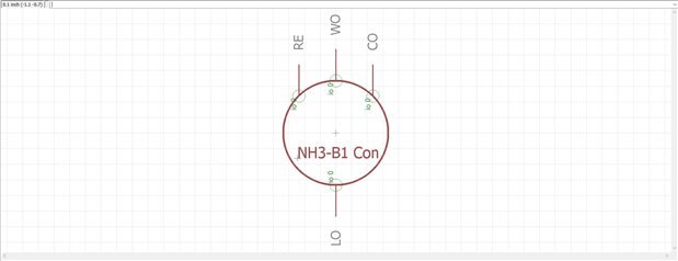
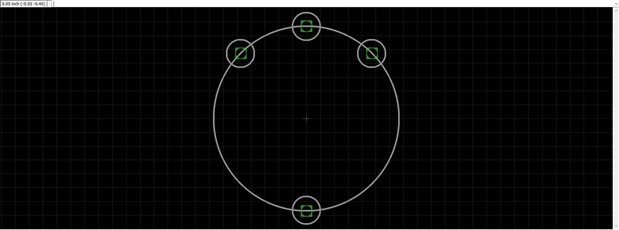
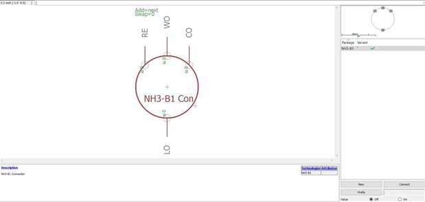
I got a problem because I can't wire to a component I created. First, I created a library for the component with Symbol, then Package and Device.
But when I am using this component on my schematic, I can't wire it. I used the same scale and grid for all the schematics and I updated libraries. But it is impossible to wire it.
If anyone has an idea to solve my problem ?