


The problem I have is described in the attached images (they are zoom-able).
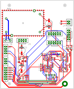
I have a finalized, fully routed design:
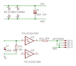
At some point I decided to add a new gate to the schematic, so I copy IC5 and paste it as IC9. Please note that no connections on IC9 have been made yet:
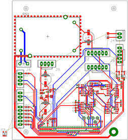
Simply placing this gate on schematic causes significant changes on the board. As you can see, multiple nets become ripped up, even the nets that have nothing to do with IC5 or IC9.
Is it possible to avoid this effect?
Thank you,
Sergey