


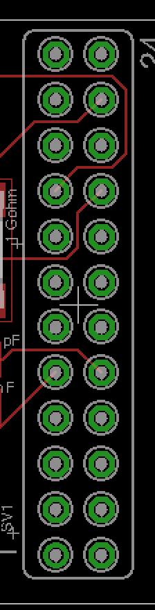
I'm new to Eagle and was looking for some help with making a PCB board layout that I will have fabricated by a board manufacturer. The goal for my project that I'm working on was to have several capacitors and resistors connected with traces to two different through-hole components, a 12x2 pin female connector (something like this: https://www.digikey.com/product-detail/en/sullins-connector-solutions/PPPC122LFBN-RC/S7115-ND/810251.)
and a right angle 3 pin connector (something like this: https://www.digikey.com/product-detail/en/sullins-connector-solutions/PPTC031LGBN-RC/S5439-ND/775897)
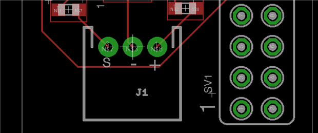
I'd like to have the pins of the connectors soldered to through holes where they connect to the traces on the top layer (ideally the only layer) of the board. The plastic of the 12x2 connector should be positioned below the top layer with the pins facing upwards, and the plastic piece of the 3 pin connector should be above the top layer of the board. I've attached a couple pictures of how I have it currently designed in my Eagle board layout.
As for my actual questions:
As it is now, I don't have any through holes that I individually placed on the board, just the through-hole components themselves, so if I sent it to a manufacturer, how would it be printed? Do I need to add another layer to the board and through-holes in order to specify more accurately how I want the board to be made, and if so, how would I do this?
Thanks in advance!

