element14 Community
element14 Community
    Register Log In
  • Site
  • Search
  • Log In Register
  • Community Hub
    Community Hub
    • What's New on element14
    • Feedback and Support
    • Benefits of Membership
    • Personal Blogs
    • Members Area
    • Achievement Levels
  • Learn
    Learn
    • Ask an Expert
    • eBooks
    • element14 presents
    • Learning Center
    • Tech Spotlight
    • STEM Academy
    • Webinars, Training and Events
    • Learning Groups
  • Technologies
    Technologies
    • 3D Printing
    • FPGA
    • Industrial Automation
    • Internet of Things
    • Power & Energy
    • Sensors
    • Technology Groups
  • Challenges & Projects
    Challenges & Projects
    • Design Challenges
    • element14 presents Projects
    • Project14
    • Arduino Projects
    • Raspberry Pi Projects
    • Project Groups
  • Products
    Products
    • Arduino
    • Avnet & Tria Boards Community
    • Dev Tools
    • Manufacturers
    • Multicomp Pro
    • Product Groups
    • Raspberry Pi
    • RoadTests & Reviews
  • About Us
  • Store
    Store
    • Visit Your Store
    • Choose another store...
      • Europe
      •  Austria (German)
      •  Belgium (Dutch, French)
      •  Bulgaria (Bulgarian)
      •  Czech Republic (Czech)
      •  Denmark (Danish)
      •  Estonia (Estonian)
      •  Finland (Finnish)
      •  France (French)
      •  Germany (German)
      •  Hungary (Hungarian)
      •  Ireland
      •  Israel
      •  Italy (Italian)
      •  Latvia (Latvian)
      •  
      •  Lithuania (Lithuanian)
      •  Netherlands (Dutch)
      •  Norway (Norwegian)
      •  Poland (Polish)
      •  Portugal (Portuguese)
      •  Romania (Romanian)
      •  Russia (Russian)
      •  Slovakia (Slovak)
      •  Slovenia (Slovenian)
      •  Spain (Spanish)
      •  Sweden (Swedish)
      •  Switzerland(German, French)
      •  Turkey (Turkish)
      •  United Kingdom
      • Asia Pacific
      •  Australia
      •  China
      •  Hong Kong
      •  India
      •  Korea (Korean)
      •  Malaysia
      •  New Zealand
      •  Philippines
      •  Singapore
      •  Taiwan
      •  Thailand (Thai)
      • Americas
      •  Brazil (Portuguese)
      •  Canada
      •  Mexico (Spanish)
      •  United States
      Can't find the country/region you're looking for? Visit our export site or find a local distributor.
  • Translate
  • Profile
  • Settings
Autodesk EAGLE
  • Products
  • More
Autodesk EAGLE
EAGLE User Support (English) Why is device footprint on board different to package footprint
  • Blog
  • Forum
  • Documents
  • Events
  • Polls
  • Files
  • Members
  • Mentions
  • Sub-Groups
  • Tags
  • More
  • Cancel
  • New
Join Autodesk EAGLE to participate - click to join for free!
Actions
  • Share
  • More
  • Cancel
Forum Thread Details
  • State Suggested Answer
  • Replies 3 replies
  • Answers 1 answer
  • Subscribers 180 subscribers
  • Views 1571 views
  • Users 0 members are here
  • eagle package
Related

Why is device footprint on board different to package footprint

onelittlegoat
onelittlegoat over 8 years ago

I have created a device and in the package editor the pad spacing looks fine, however, when I place the device onto the circuit board, the dimensions look different and the pads are way closer together.


It is definitely the same package because I can right click the device on the board and go Open Package and it opens the package but it looks different.  The drill size and diameter size has been set manually in the package for all the pins.


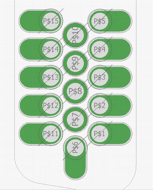
Here is what it looks like in the package editor.  Looks fine.


image


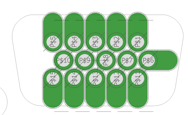
...and here is the footprint when placed on the circuit board, everything is fatter.


image


Shouldn't they display the same?


Phil

  • Sign in to reply
  • Cancel
  • autodeskguest
    0 autodeskguest over 8 years ago

    Eagle is behaving correctly and this would be the most ask question.

    So go to the FAQ


    How to Define the Pad Diameter?


    https://knowledge.autodesk.com/support/eagle/learn-explore/caas/simplecontent/content/autodesk-eagle-frequently-asked-questions.html#22


    Hope this gets you started.


    Search for this subject in the forums and you will find further

    postings/information on settings for your DRC that can give you more

    control.


    All the best

    Warren

    --

    EAGLE support forums at http://www.eaglecentral.ca :: Where the EAGLE community meets.


    • Cancel
    • Vote Up 0 Vote Down
    • Sign in to reply
    • Verify Answer
    • Cancel
  • jltharin
    0 jltharin over 8 years ago in reply to autodeskguest

    Hi Philip

    In DRC, some options can modify the shape of pads

    Below you can see where, check this option are "As library"


    image

    image

    Hope this can help you


    jltharin

    • Cancel
    • Vote Up 0 Vote Down
    • Sign in to reply
    • Verify Answer
    • Cancel
  • rachaelp
    0 rachaelp over 8 years ago in reply to jltharin

    jltharin  wrote:


    In DRC, some options can modify the shape of pads

    Hi Jltharin,


    Those are good points and show some of the things which can cause a discrepancy. You've actually missed one off though, and it's the one that's actually causing the issue in this case. The "Restring" settings actually modify the size of the pads which if you look at the images in the original post you can see that the pads have increased in size in the board. This is because the pads in the library were smaller than the minimum calculation made by the restring setting so it increased them automatically.


    Anyway, as this post is over a month old I suspect Philip may have found his answer elsewhere as he's not been back on the thread but it was good to post the answers up for completeness in case anybody stumbles across this thread in future. Thanks!


    Best Regards,


    Rachael

    • Cancel
    • Vote Up 0 Vote Down
    • Sign in to reply
    • Verify Answer
    • Reject Answer
    • Cancel
element14 Community

element14 is the first online community specifically for engineers. Connect with your peers and get expert answers to your questions.

  • Members
  • Learn
  • Technologies
  • Challenges & Projects
  • Products
  • Store
  • About Us
  • Feedback & Support
  • FAQs
  • Terms of Use
  • Privacy Policy
  • Legal and Copyright Notices
  • Sitemap
  • Cookies

An Avnet Company © 2025 Premier Farnell Limited. All Rights Reserved.

Premier Farnell Ltd, registered in England and Wales (no 00876412), registered office: Farnell House, Forge Lane, Leeds LS12 2NE.

ICP 备案号 10220084.

Follow element14

  • X
  • Facebook
  • linkedin
  • YouTube