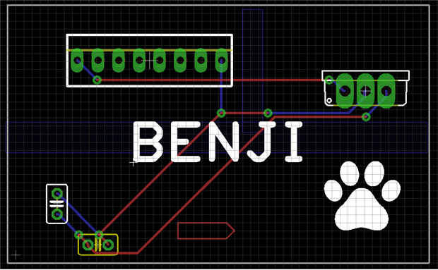
As a hobbyist, I find it much faster for prototyping make my own boards and recently got a CNC router to speed up prototyping. I usually route the boards myself but sometimes don't have enough time to do it by hand. The problem is that while the auto-router works fine for hand-made single sided boards, for double-sided boards, there is no way to turn off PTH for the pads. It will always assume the top and bottom of all pads to be connected by default and route accordingly. As everyone knows, making PTH at home is not feasible(time and money).
Is there any setting to tell the auto-router not to assume pads' top and bottom to be connected?
One way I see is by using a ULP that places pads' duplicate shapes on bRestrict for parts on bottom side and on tRestrict for parts on the top side. Is there any such ULP available?