element14 Community
element14 Community
    Register Log In
  • Site
  • Search
  • Log In Register
  • About Us
  • Community Hub
    Community Hub
    • What's New on element14
    • Feedback and Support
    • Benefits of Membership
    • Personal Blogs
    • Members Area
    • Achievement Levels
  • Learn
    Learn
    • Ask an Expert
    • eBooks
    • element14 presents
    • Learning Center
    • Tech Spotlight
    • STEM Academy
    • Webinars, Training and Events
    • Learning Groups
  • Technologies
    Technologies
    • 3D Printing
    • FPGA
    • Industrial Automation
    • Internet of Things
    • Power & Energy
    • Sensors
    • Technology Groups
  • Challenges & Projects
    Challenges & Projects
    • Design Challenges
    • element14 presents Projects
    • Project14
    • Arduino Projects
    • Raspberry Pi Projects
    • Project Groups
  • Products
    Products
    • Arduino
    • Avnet Boards Community
    • Dev Tools
    • Manufacturers
    • Multicomp Pro
    • Product Groups
    • Raspberry Pi
    • RoadTests & Reviews
  • Store
    Store
    • Visit Your Store
    • Choose another store...
      • Europe
      •  Austria (German)
      •  Belgium (Dutch, French)
      •  Bulgaria (Bulgarian)
      •  Czech Republic (Czech)
      •  Denmark (Danish)
      •  Estonia (Estonian)
      •  Finland (Finnish)
      •  France (French)
      •  Germany (German)
      •  Hungary (Hungarian)
      •  Ireland
      •  Israel
      •  Italy (Italian)
      •  Latvia (Latvian)
      •  
      •  Lithuania (Lithuanian)
      •  Netherlands (Dutch)
      •  Norway (Norwegian)
      •  Poland (Polish)
      •  Portugal (Portuguese)
      •  Romania (Romanian)
      •  Russia (Russian)
      •  Slovakia (Slovak)
      •  Slovenia (Slovenian)
      •  Spain (Spanish)
      •  Sweden (Swedish)
      •  Switzerland(German, French)
      •  Turkey (Turkish)
      •  United Kingdom
      • Asia Pacific
      •  Australia
      •  China
      •  Hong Kong
      •  India
      •  Korea (Korean)
      •  Malaysia
      •  New Zealand
      •  Philippines
      •  Singapore
      •  Taiwan
      •  Thailand (Thai)
      • Americas
      •  Brazil (Portuguese)
      •  Canada
      •  Mexico (Spanish)
      •  United States
      Can't find the country/region you're looking for? Visit our export site or find a local distributor.
  • Translate
  • Profile
  • Settings
Autodesk EAGLE
  • Products
  • More
Autodesk EAGLE
EAGLE User Support (English) Kelvin connection in Eagle
  • Blog
  • Forum
  • Documents
  • Events
  • Polls
  • Files
  • Members
  • Mentions
  • Sub-Groups
  • Tags
  • More
  • Cancel
  • New
Join Autodesk EAGLE to participate - click to join for free!
Actions
  • Share
  • More
  • Cancel
Forum Thread Details
  • State Verified Answer
  • Replies 8 replies
  • Answers 4 answers
  • Subscribers 177 subscribers
  • Views 3167 views
  • Users 0 members are here
  • eagle
  • kelvin_resistor
  • eagle_cad
  • custom pcb
Related

Kelvin connection in Eagle

jjvan
jjvan over 6 years ago

Hey everyone!


I'm still learning eagle, so some obvious things are still difficult for me to wrap my head around, but I'm learning!


I have a question regarding Kelvin connections in Eagle. I have a board I need to design that performs current sensing. It has 2 input jacks, 2 output bnc jacks (that go to a differential amplifier) and a shunt resistor to measure the voltage drop across. My supervisor has asked me to implement the following pad layout for the kelvin connection with this shunt resistor: https://www.bourns.com/docs/Product-Datasheets/css2h-2512.pdf

image

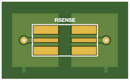
To do this the only approach I could come up with was to design a new footprint for the shunt resistor in which both sides have 3 pads. So I came up with this footprint (Bourns_CSS2H-2512-A in this library: https://github.com/joshvandermeer/Eaglelibrary )


image

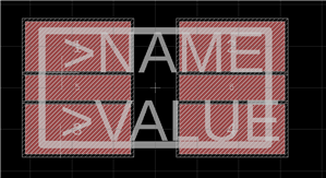
Then when I try to connect to the pads manually using the polygon tool in eagle, I get the following:

image

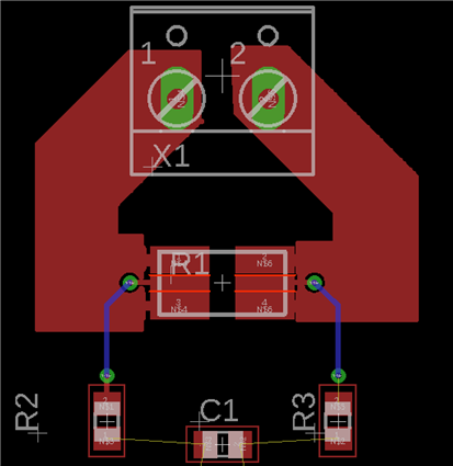
Where it looks like each pad has a maximum trace width for the trace connecting to it. This circuit will have a high current, so I want the traces to connect completely, not just by a thin trace at the terminals.


Is there anything I can do to improve this situation? I'm new to this, so I'm sure I'm overlooking something important, and I really appreciate any advice!


Thank you!

  • Sign in to reply
  • Cancel

Top Replies

  • autodeskguest
    autodeskguest over 6 years ago in reply to rachaelp +3 suggested
    On 15.10.2018 11:01, rachaelp wrote: wrote: I think you are way overdoing this circuit, and at the same time you weaken it. If the resistor is tightly dimensioned for your power, you need the full pad…
  • rachaelp
    rachaelp over 6 years ago +2 verified
    Hi Joshua, It looks like there are more issues than just your connection widths. If you look you actually have the signal polygon fills shorting with your sense trace. You need to do your footprint and…
  • rachaelp
    rachaelp over 6 years ago in reply to autodeskguest +2 suggested
    autodeskguest wrote: I think you are way overdoing this circuit, and at the same time you weaken it. If the resistor is tightly dimensioned for your power, you need the full pad both for heatsink and current…
  • rachaelp
    0 rachaelp over 6 years ago

    Hi Joshua,


    It looks like there are more issues than just your connection widths. If you look you actually have the signal polygon fills shorting with your sense trace. You need to do your footprint and your schematic symbol to allow the 4 terminal connection. So on each side the two outer pad pieces connect to the corresponding main resistor pin and the central pad connects to a separate current sense pin with a separately named net. I'm at work at the moment so can't explain further but if you are still having issues I will try and explain better later.


    With regards to the connection, turn off thermals for the polygon and then it will connect fully.


    Best Regards,


    Rachael

    • Cancel
    • Vote Up +2 Vote Down
    • Sign in to reply
    • Verify Answer
    • Reject Answer
    • Cancel
  • jjvan
    0 jjvan over 6 years ago in reply to rachaelp

    Rachael,


    Thank you! Ya I fumbled around with it more and improved the resistor footprint to have pads better defined and that helped fix my problem. I'm just getting started with Eagle so I'm learning all the intricacies of how to properly create a part.

    • Cancel
    • Vote Up +1 Vote Down
    • Sign in to reply
    • Verify Answer
    • Cancel
  • autodeskguest
    0 autodeskguest over 6 years ago

    On 08.10.2018 17:06, Joshua Vandermeer wrote:

    Hey everyone!


    I'm still learning eagle, so some obvious things are still difficult for me to wrap my head around, but I'm learning!


    I think you are way overdoing this circuit, and at the same time you

    weaken it. If the resistor is tightly dimensioned for your power, you

    need the full pad both for heatsink and current.


    Just route the kelvin probes out on the side of the SMD pads. The point

    of the kelvin probes are to avoid the voltage drop in the high current

    main path. If you just bring out some probes on the side of the smd's,

    there will be close to no current generating voltage drop on those

    tracks. If you want max noise immunity, route the two tracks

    differential back to the sensing circuit. For even more noise immunity

    route them through directly down a VIA to a different opposite layer.


    The implementation of the kelvin probes is done at the board layouyt,

    not the schematic, but if you need others to do the routing job based on

    your schematic drawings, draw it like you would route it and put a

    comment in the schematic at the info or guide layer.


    • Cancel
    • Vote Up +1 Vote Down
    • Sign in to reply
    • Verify Answer
    • Reject Answer
    • Cancel
  • rachaelp
    0 rachaelp over 6 years ago in reply to autodeskguest

    autodeskguest  wrote:


    I think you are way overdoing this circuit, and at the same time you

    weaken it. If the resistor is tightly dimensioned for your power, you

    need the full pad both for heatsink and current.


    Just route the kelvin probes out on the side of the SMD pads.


    Joshua does say in his first post "My supervisor has asked me to implement the following pad layout for the kelvin connection with this shunt resistor". It might not be what you would do, but it is what he was asked to implement by his supervisor.


    Best Regards,


    Rachael

    • Cancel
    • Vote Up +2 Vote Down
    • Sign in to reply
    • Verify Answer
    • Reject Answer
    • Cancel
  • autodeskguest
    0 autodeskguest over 6 years ago in reply to rachaelp

    On 15.10.2018 11:01, rachaelp wrote:

      wrote:


    I think you are way overdoing this circuit, and at the same time you

    weaken it. If the resistor is tightly dimensioned for your power, you

    need the full pad both for heatsink and current.


    Just route the kelvin probes out on the side of the SMD pads.


    Joshua does say in his first post "My supervisor has asked me to implement the following pad layout for the kelvin connection with this shunt resistor". It might not be what you would do, but it is what he was asked to implement by his supervisor.


    Best Regards,


    Rachael


    Fair enough Rachael image


    If this was me, I would go back to my supervisor and demonstrate my

    skills and tell him about this implementations weakness but it may not

    be the right thing for Joshua this time. That's up to him.


    To add more feedback to his supervisor, Im not even sure if a

    manufacturer would like this implementation, due to it's potential

    bistable nature. When the lead melts, this got a bistable nature of not

    falling to rest on the large pads, but may be pulled to one side or the

    other.


    • Cancel
    • Vote Up +3 Vote Down
    • Sign in to reply
    • Verify Answer
    • Reject Answer
    • Cancel
  • jjvan
    0 jjvan over 6 years ago in reply to autodeskguest

    Thank you both for the great advice. I agree that the implementation I was shooting for was very overcomplicated. I'm an intern right now and trying to take as much instruction as I can. I was given this document to follow, but there was a miscommunication and he just wanted me to learn from it, not actually implement it.


    Optimize High-Current Sensing Accuracy by Improving Pad Layout of Low-Value Shunt Resistors | Analog Devices


    Ended up just taking the kelvin connection from the inside of the pads.

    • Cancel
    • Vote Up +1 Vote Down
    • Sign in to reply
    • Verify Answer
    • Cancel
  • autodeskguest
    0 autodeskguest over 6 years ago in reply to jjvan

    On 15.10.2018 17:19, Joshua Vandermeer wrote:

    Thank you both for the great advice. I agree that the implementation I was shooting for was very overcomplicated. I'm an intern right now and trying to take as much instruction as I can. I was given this document to follow, but there was a miscommunication and he just wanted me to learn from it, not actually implement it.


    Optimize High-Current Sensing Accuracy by Improving Pad Layout of Low-Value Shunt Resistors | Analog Devices (http://www.analog.com/en/analog-dialogue/articles/optimize-high-current-sensing-accuracy.html)


    Ended up just taking the kelvin connection from the inside of the pads.


    Interesting experiment there.. Using constant current source may not

    reveal all the weaknesses tho. Voltage applied to get to that current

    may vary to compensate higher R(solder) on the smaller area pads, and

    this may cause undesired effects. Also thermal effects may increase

    because of the same problem.


    Your conclusion seem to be something what I would do, but this is very

    dependant on how the resistor is actually built. Choosing the shortest

    path to the actual start of the resistor material would give best result.


    Because of the resistor physics, you could also analyze the result on

    different fine tuned positions of the resistor, but these are errors

    that are hard to control in mass production.


    If you really would need a high precision, high yield kelvin probe, some

    extra attention to all the side effects may be required, but usually you

    end up with some calibration process. This is why noise is more of a

    real problem than offset errors.


    • Cancel
    • Vote Up +1 Vote Down
    • Sign in to reply
    • Verify Answer
    • Reject Answer
    • Cancel
  • autodeskguest
    0 autodeskguest over 6 years ago in reply to autodeskguest

    I had a similar need.


    What I ended up doing was to create a net class with special trace widths different from the rest on the board. THen When this is autorouted it always is routed directly to where it should be, nothing shared.


    --

    To view any images and attachments in this post, visit:

    https://www.element14.com/community/message/277798


    • Cancel
    • Vote Up 0 Vote Down
    • Sign in to reply
    • Verify Answer
    • Cancel
element14 Community

element14 is the first online community specifically for engineers. Connect with your peers and get expert answers to your questions.

  • Members
  • Learn
  • Technologies
  • Challenges & Projects
  • Products
  • Store
  • About Us
  • Feedback & Support
  • FAQs
  • Terms of Use
  • Privacy Policy
  • Legal and Copyright Notices
  • Sitemap
  • Cookies

An Avnet Company © 2025 Premier Farnell Limited. All Rights Reserved.

Premier Farnell Ltd, registered in England and Wales (no 00876412), registered office: Farnell House, Forge Lane, Leeds LS12 2NE.

ICP 备案号 10220084.

Follow element14

  • X
  • Facebook
  • linkedin
  • YouTube