Hi All,
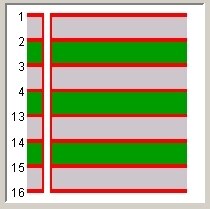
Im trying to create an 8 Layer PCB stackup I want to follow the best practices and I fond this site: http://www.hottconsultants.com along with many other that say that my 8 layer board stackup should be make like this (for better EMC and signal integrity)
~~~~~~~~~~~~~~~ Mounting Pads/Low Freq. Signals
::::::::::::::: Prepreg
+++++++++++++++ Pwr.
=============== FR4 Core
--------------- Gnd.
::::::::::::::: Prepreg
~~~~~~~~~~~~~~~ High Freq. Signals
=============== FR4 Core
~~~~~~~~~~~~~~~ High Freq. Signals
::::::::::::::: Prepreg
--------------- Gnd.
=============== FR4 Core
+++++++++++++++ Pwr.
::::::::::::::: Prepreg
~~~~~~~~~~~~~~~ Low Freq. Signals/Test Pads
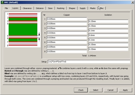
I've never worked with eagle with so many layers, and never even bother with blind and burried vias.
I need some help to define this stackup in eagle and also to create the throu, burried and blind vias to connect the layers.
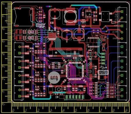
This is the very basic stackup I've with no vias 
Thanks in advance.
Ben.