element14 Community
element14 Community
    Register Log In
  • Site
  • Search
  • Log In Register
  • Community Hub
    Community Hub
    • What's New on element14
    • Feedback and Support
    • Benefits of Membership
    • Personal Blogs
    • Members Area
    • Achievement Levels
  • Learn
    Learn
    • Ask an Expert
    • eBooks
    • element14 presents
    • Learning Center
    • Tech Spotlight
    • STEM Academy
    • Webinars, Training and Events
    • Learning Groups
  • Technologies
    Technologies
    • 3D Printing
    • FPGA
    • Industrial Automation
    • Internet of Things
    • Power & Energy
    • Sensors
    • Technology Groups
  • Challenges & Projects
    Challenges & Projects
    • Design Challenges
    • element14 presents Projects
    • Project14
    • Arduino Projects
    • Raspberry Pi Projects
    • Project Groups
  • Products
    Products
    • Arduino
    • Avnet & Tria Boards Community
    • Dev Tools
    • Manufacturers
    • Multicomp Pro
    • Product Groups
    • Raspberry Pi
    • RoadTests & Reviews
  • About Us
    About the element14 Community
  • Store
    Store
    • Visit Your Store
    • Choose another store...
      • Europe
      •  Austria (German)
      •  Belgium (Dutch, French)
      •  Bulgaria (Bulgarian)
      •  Czech Republic (Czech)
      •  Denmark (Danish)
      •  Estonia (Estonian)
      •  Finland (Finnish)
      •  France (French)
      •  Germany (German)
      •  Hungary (Hungarian)
      •  Ireland
      •  Israel
      •  Italy (Italian)
      •  Latvia (Latvian)
      •  
      •  Lithuania (Lithuanian)
      •  Netherlands (Dutch)
      •  Norway (Norwegian)
      •  Poland (Polish)
      •  Portugal (Portuguese)
      •  Romania (Romanian)
      •  Russia (Russian)
      •  Slovakia (Slovak)
      •  Slovenia (Slovenian)
      •  Spain (Spanish)
      •  Sweden (Swedish)
      •  Switzerland(German, French)
      •  Turkey (Turkish)
      •  United Kingdom
      • Asia Pacific
      •  Australia
      •  China
      •  Hong Kong
      •  India
      •  Japan
      •  Korea (Korean)
      •  Malaysia
      •  New Zealand
      •  Philippines
      •  Singapore
      •  Taiwan
      •  Thailand (Thai)
      •  Vietnam
      • Americas
      •  Brazil (Portuguese)
      •  Canada
      •  Mexico (Spanish)
      •  United States
      Can't find the country/region you're looking for? Visit our export site or find a local distributor.
  • Translate
  • Profile
  • Settings
Autodesk EAGLE
  • Products
  • More
Autodesk EAGLE
EAGLE User Support (English) How can I make a large 0.900 in (23mm) pad diameter for a wirepad?
  • Blog
  • Forum
  • Documents
  • Events
  • Polls
  • Files
  • Members
  • Mentions
  • Sub-Groups
  • Tags
  • More
  • Cancel
  • New
Join Autodesk EAGLE to participate - click to join for free!
Actions
  • Share
  • More
  • Cancel
Forum Thread Details
  • State Verified Answer
  • Replies 8 replies
  • Subscribers 188 subscribers
  • Views 1099 views
  • Users 0 members are here
Related

How can I make a large 0.900 in (23mm) pad diameter for a wirepad?

e14 Contributor
e14 Contributor over 15 years ago

Hello:
I  am trying make a large pad diameter of 0.900 inches, and maximum pad  dia. allowed in Eagle is only 0.51 inches. Is there a work around, or  another way to get a large pad size?


I tried making a circle on the same layer as the maximum allowed pad (Pads) that overlapped the pad, but that did not work: It would not connect to a copper pour polygon of the same net name.


Thanks for the help!
Tim

  • Sign in to reply
  • Cancel
  • e14 Contributor
    0 e14 Contributor over 15 years ago in reply to e14 Contributor

    THANKS SO MUCH!!

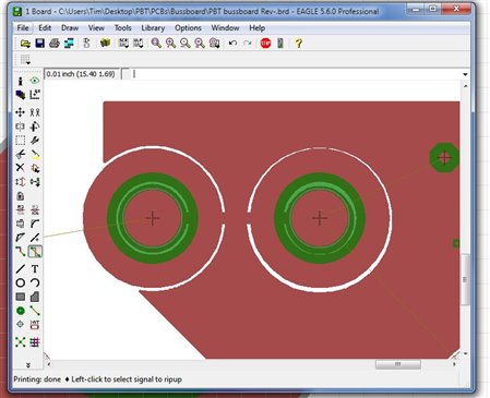
    In the attached graphic you will see the work around. A polygon can be used but not arcs or circles (strangely enough!).


    So thanks again both of you, really appreciate having a new library item for my large pad!image

    Tim

    • Cancel
    • Vote Up 0 Vote Down
    • Sign in to reply
    • Verify Answer
    • Cancel
  • e14 Contributor
    0 e14 Contributor over 15 years ago in reply to e14 Contributor

    THanks very much for all your help.

    I'm using EAGLE Version 5.6.0 for Windows and I'd like to have a library part

    for a wirepad that is larger than .5 inch. I'll try Pauls technique with the stop mask,

    maybe that is my problem. Thanks again!

    • Cancel
    • Vote Up 0 Vote Down
    • Sign in to reply
    • Verify Answer
    • Cancel
  • e14 Contributor
    0 e14 Contributor over 15 years ago in reply to e14 Contributor

    Tim Economu schrieb:


    a), I really have absolutely no idea what you mean. I have been using

    Eagle for maybe 6 or 7 years now, and really never needed much

    support until now.


    You are posting via element14, which is just a web based gateway to the

    newsgroups, where the discussions originate. Sadly, this gateway doesn't

    work correct, so any image you are posting there does not appear at the

    newsgroups. There is another web gateway at eaglecentral.ca, which works

    significantly better. The majority of posters uses the newsgroups or

    that other gateway, so your image is visible only for a small part of

    the users.


    I recommend having a look at direct newsgroup access (with a decent

    newsreader) or at the webgate at eaglecentral.ca.


    b) I am asking about how to build a pad larger than the Eagle default

    of 1/2 inch. That is (as far as I know) only possible in the library.

    As I said I tryed using two arcs to define a larger pad, on top of

    the existing .5 inch pad, and as the image shows, the copper polygon

    pour will not connect to the new copper pad. If I delete the "new"

    larger pad made of arcs, the existing .5 in pad 'will' connect to the

    pour.


    As Paul already asked: maybe you are working with an older version of

    EAGLE? Then you should create your larger "pad" directly within the

    board. Even if it's part of some package definition - you can put the

    hole and the stop masks in the package, then add the required copper

    directly in the board using a polygon (and/or two ARCs of proper width,

    if you need copper up to the hole for plating-through).


    Tilmann


    • Cancel
    • Vote Up 0 Vote Down
    • Sign in to reply
    • Verify Answer
    • Cancel
  • e14 Contributor
    0 e14 Contributor over 15 years ago in reply to e14 Contributor

    On 08/31/2011 07:17 PM, Tim Economu wrote:

    Thanks again for the help Tilmann,

    About your answers,

    a), I really have absolutely no idea what you mean. I have been using Eagle for maybe 6 or 7 years now, and really never needed much support until now.

    b) I am asking about how to build a pad larger than the Eagle default of 1/2 inch. That is (as far as I know) only possible in the library.  As I said I tryed using two arcs to define a larger pad, on top of the existing .5 inch pad, and as the image shows, the copper polygon pour will not connect to the new copper pad. If I delete the "new" larger pad made of arcs, the existing .5 in pad 'will' connect to the pour.


    I find it hard to believe there is no easy way to get a larger than 0.5 inch wirepad in Eagle!!


    Thanks,

    Tim


    Eagle version???

    with 4.1x you can't really add copper to lib's. With 5.+ I think you can

    but I never upgraded.

    With eagle 5.+ in the lib make a square polygon and then round with the

    miter tool.


    With 4.1x fix the stop mask to the larger size then use a named polygon

    on the board.


    Paul R.


    • Cancel
    • Vote Up 0 Vote Down
    • Sign in to reply
    • Reject Answer
    • Cancel
  • e14 Contributor
    0 e14 Contributor over 15 years ago in reply to e14 Contributor

    Thanks again for the help Tilmann,

    About your answers,

    a), I really have absolutely no idea what you mean. I have been using Eagle for maybe 6 or 7 years now, and really never needed much support until now.

    b) I am asking about how to build a pad larger than the Eagle default of 1/2 inch. That is (as far as I know) only possible in the library.  As I said I tryed using two arcs to define a larger pad, on top of the existing .5 inch pad, and as the image shows, the copper polygon pour will not connect to the new copper pad. If I delete the "new" larger pad made of arcs, the existing .5 in pad 'will' connect to the pour.


    I find it hard to believe there is no easy way to get a larger than 0.5 inch wirepad in Eagle!!


    Thanks,

    Tim

    • Cancel
    • Vote Up 0 Vote Down
    • Sign in to reply
    • Verify Answer
    • Cancel
  • e14 Contributor
    0 e14 Contributor over 15 years ago in reply to e14 Contributor

    Tim Economu schrieb:


    Thanks Tilman, I tried your method, in the library editor, I made

    two 180 degree arcs on the top copper layer overlapping the pad on

    the pad layer. Trying to put a copper polygon pour of the same net

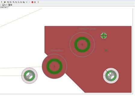
    name in board layout unfortunately  Image:padnotconnectedtopour.JPG

    does not connect the new copper arc pads to the top copper polygon.


    a) If you put images in that badly broken webgate, they never appear in

    the original newsgroups or in the other (significantly better working)

    webgate.


    b) You didn't mention before that you want to do this within a library

    (i.e. package). The method I described is fine directly in the board. In

    a package, you better draw a round-appearing polygon (outlines also

    built with two ARCs). It will be "merged" with an SMD pad inside (that

    you need for defining the connections).


    Tilmann


    • Cancel
    • Vote Up 0 Vote Down
    • Sign in to reply
    • Verify Answer
    • Cancel
  • e14 Contributor
    0 e14 Contributor over 15 years ago in reply to e14 Contributor

    Thanks Tilman,

    I tried your method, in the library editor, I made two 180 degree arcs on the top copper layer overlapping the pad on the pad layer.

    Trying to put a copper polygon pour of the same net name in board layout unfortunately does not connect the new copper arc pads to the top copper polygon.image

    I can connect with a trace of course, and simulate a thermal on the pour by hand, but I would like the new pad to look just like a regular pad and connnect to the pour with thermals or without thermals, either way would be fine.

    • Cancel
    • Vote Up 0 Vote Down
    • Sign in to reply
    • Verify Answer
    • Cancel
  • e14 Contributor
    0 e14 Contributor over 15 years ago

    Tim Economu schrieb:


    I  am trying make a large pad diameter of 0.900 inches, and maximum

    pad  dia. allowed in Eagle is only 0.51 inches. Is there a work

    around, or  another way to get a large pad size?


    I tried making a circle on the same layer as the maximum allowed pad

    (Pads) that overlapped the pad, but that did not work: It would not

    connect to a copper pour polygon of the same net name.


    Don't draw into the PADS layer, draw into the copper layer(s).


    Then, a circle cannot be assigned to a signal - but ARCs can, simply use

    two arcs of (say) 180° each.


    Tilmann


    • Cancel
    • Vote Up 0 Vote Down
    • Sign in to reply
    • Verify Answer
    • Cancel
element14 Community

element14 is the first online community specifically for engineers. Connect with your peers and get expert answers to your questions.

  • Members
  • Learn
  • Technologies
  • Challenges & Projects
  • Products
  • Store
  • About Us
  • Feedback & Support
  • FAQs
  • Terms of Use
  • Privacy Policy
  • Legal and Copyright Notices
  • Sitemap
  • Cookies

An Avnet Company © 2026 Premier Farnell Limited. All Rights Reserved.

Premier Farnell Ltd, registered in England and Wales (no 00876412), registered office: Farnell House, Forge Lane, Leeds LS12 2NE.

Follow element14

  • X
  • Facebook
  • linkedin
  • YouTube