element14 Community
element14 Community
    Register Log In
  • Site
  • Search
  • Log In Register
  • Community Hub
    Community Hub
    • What's New on element14
    • Feedback and Support
    • Benefits of Membership
    • Personal Blogs
    • Members Area
    • Achievement Levels
  • Learn
    Learn
    • Ask an Expert
    • eBooks
    • element14 presents
    • Learning Center
    • Tech Spotlight
    • STEM Academy
    • Webinars, Training and Events
    • Learning Groups
  • Technologies
    Technologies
    • 3D Printing
    • FPGA
    • Industrial Automation
    • Internet of Things
    • Power & Energy
    • Sensors
    • Technology Groups
  • Challenges & Projects
    Challenges & Projects
    • Design Challenges
    • element14 presents Projects
    • Project14
    • Arduino Projects
    • Raspberry Pi Projects
    • Project Groups
  • Products
    Products
    • Arduino
    • Avnet Boards Community
    • Dev Tools
    • Manufacturers
    • Multicomp Pro
    • Product Groups
    • Raspberry Pi
    • RoadTests & Reviews
  • Store
    Store
    • Visit Your Store
    • Choose another store...
      • Europe
      •  Austria (German)
      •  Belgium (Dutch, French)
      •  Bulgaria (Bulgarian)
      •  Czech Republic (Czech)
      •  Denmark (Danish)
      •  Estonia (Estonian)
      •  Finland (Finnish)
      •  France (French)
      •  Germany (German)
      •  Hungary (Hungarian)
      •  Ireland
      •  Israel
      •  Italy (Italian)
      •  Latvia (Latvian)
      •  
      •  Lithuania (Lithuanian)
      •  Netherlands (Dutch)
      •  Norway (Norwegian)
      •  Poland (Polish)
      •  Portugal (Portuguese)
      •  Romania (Romanian)
      •  Russia (Russian)
      •  Slovakia (Slovak)
      •  Slovenia (Slovenian)
      •  Spain (Spanish)
      •  Sweden (Swedish)
      •  Switzerland(German, French)
      •  Turkey (Turkish)
      •  United Kingdom
      • Asia Pacific
      •  Australia
      •  China
      •  Hong Kong
      •  India
      •  Korea (Korean)
      •  Malaysia
      •  New Zealand
      •  Philippines
      •  Singapore
      •  Taiwan
      •  Thailand (Thai)
      • Americas
      •  Brazil (Portuguese)
      •  Canada
      •  Mexico (Spanish)
      •  United States
      Can't find the country/region you're looking for? Visit our export site or find a local distributor.
  • Translate
  • Profile
  • Settings
Autodesk EAGLE
  • Products
  • More
Autodesk EAGLE
EAGLE User Support (English) Make PCB etched route wider?
  • Blog
  • Forum
  • Documents
  • Events
  • Polls
  • Files
  • Members
  • Mentions
  • Sub-Groups
  • Tags
  • More
  • Cancel
  • New
Join Autodesk EAGLE to participate - click to join for free!
Actions
  • Share
  • More
  • Cancel
Forum Thread Details
  • State Verified Answer
  • Replies 7 replies
  • Subscribers 173 subscribers
  • Views 1730 views
  • Users 0 members are here
Related

Make PCB etched route wider?

velocity
velocity over 11 years ago

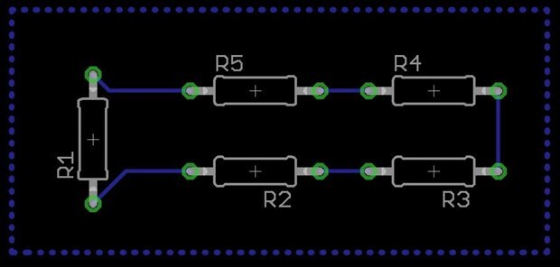
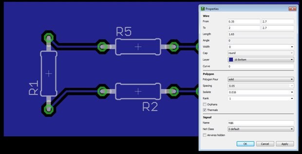
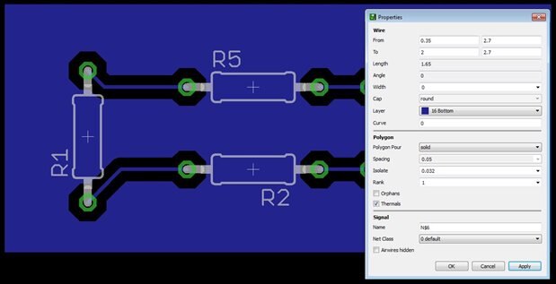
Hello everyone,  I'm new to Eagle Cad and was wondering if anyone could give me a tip on widening the etched route lines when I go to make a PCB layout.  I'm not referring to the actual traces but the lines that my CNC machine would etch out the copper during milling.  Problem is that the smallest endmill I have is a 1mm and when I go to process the G-Code, it fails because the etch lines are smaller than my endmill.  Any help would be very much appreciated!  Thanks!


image

  • Sign in to reply
  • Cancel
  • Former Member
    0 Former Member over 11 years ago

    Hello Nick Knack,

    It looks like you'll need to change the distance settings for when the copper pour/flood is generated.

    In the PCB editor you can go to Edit->Design Rules; select the 'Distance' tab in the window which opens.

    image

    Now if you set the value Copper/Dimension to 1mm and then 'OK', next re-pour your polygon and you should find 1mm gap has been generated.

    HTH.


    <edit> From the built in help:-

    "Isolate

    Distance between polygon areas and other signals or objects in the Dimension layer (default: 0). If a particular polygon is given an Isolate value that exceeds that from the design rules and net classes, the larger value will be taken. See also Design Rules under Distance and Supply, respectively. Note that if you give a polygon an Isolate value that exceeds that from the design rules and net classes, small gaps may result between the calculated polygon and objects belonging to the same signal as the polygon itself, which may lead to problems during manufacturing! It is therefore recommended to leave this parameter at 0, unless you know exactly what you are doing!"

    </edit>

    • Cancel
    • Vote Up 0 Vote Down
    • Sign in to reply
    • Verify Answer
    • Cancel
  • GRPZijlstra
    0 GRPZijlstra over 11 years ago

    Hello.


    The distance between the edge of the trace and the edge of the copper pour is the isolation parameter of the polygon you drew for the copper pour.


    Either change it using the Change icon, set isolation to whatever you need and click the polygon.

    Or right-click on the polygon, select properties and set the isolation to the width you require.


    Hope this helps,

    Guido

    • Cancel
    • Vote Up 0 Vote Down
    • Sign in to reply
    • Verify Answer
    • Cancel
  • velocity
    0 velocity over 11 years ago

    Hi guys,


    Thanks for the replies.  I went through and tried what you advised but all it does is thicken the trace and not the etched lines (the lines that show up black) -- which would be the lines that are milled by the CNC endmill (see image).


    image

    • Cancel
    • Vote Up 0 Vote Down
    • Sign in to reply
    • Verify Answer
    • Cancel
  • Former Member
    0 Former Member over 11 years ago in reply to velocity

    What version of Eagle are you using?

    Would you be happy to attach your .pcb file for me to have a look myself?

    ATB,

    • Cancel
    • Vote Up 0 Vote Down
    • Sign in to reply
    • Verify Answer
    • Cancel
  • Former Member
    0 Former Member over 11 years ago in reply to velocity

    Hi Nick.

    You must go back to the Width of the trace between C10 and R8, by use of 'Change' - Width - select a value. Then click the very thick tracks.

    The information you got should be 'Clearance', in tools - DRC.

    HTH

    Mogens

    • Cancel
    • Vote Up 0 Vote Down
    • Sign in to reply
    • Verify Answer
    • Cancel
  • GRPZijlstra
    0 GRPZijlstra over 11 years ago in reply to velocity

    That is weird. I made a few screenshots.

    image

    I made this simple board with some normal .016 inch traces. The dotted line is the plygon for the copper-pour (ground pour).


    I then hit the ratsnest icon to get the plygon filled using standard .016 inch isolation :

    image

    I then selected the polygon (either right-click -> properties or using the 'i' icon) and changed the isolate to 0.032 :

    image

    As you can see this should do what you need (unless the blue plane in your board is not done using a polygon with copper-pour, but it looks like it is).


    Of course, the distance between normal traces (not between a trace and a copper-pour/plane) is controlled by you if you route manually, or by the clearance parameter in the DRC settings when using the autorouter as Mogens indicated.


    Hope this helps,

    Guido

    • Cancel
    • Vote Up 0 Vote Down
    • Sign in to reply
    • Reject Answer
    • Cancel
  • velocity
    0 velocity over 11 years ago in reply to GRPZijlstra

    Thank you, Guido! (and everyone else as well) That was the ticket!  My issue was that I was right-clicking the properties for the trace and not for the polygon.  Once you showed me your screenshots, I figured it out and it works great now!


    Thanks so much!

    • Cancel
    • Vote Up 0 Vote Down
    • Sign in to reply
    • Verify Answer
    • Cancel
element14 Community

element14 is the first online community specifically for engineers. Connect with your peers and get expert answers to your questions.

  • Members
  • Learn
  • Technologies
  • Challenges & Projects
  • Products
  • Store
  • About Us
  • Feedback & Support
  • FAQs
  • Terms of Use
  • Privacy Policy
  • Legal and Copyright Notices
  • Sitemap
  • Cookies

An Avnet Company © 2025 Premier Farnell Limited. All Rights Reserved.

Premier Farnell Ltd, registered in England and Wales (no 00876412), registered office: Farnell House, Forge Lane, Leeds LS12 2NE.

ICP 备案号 10220084.

Follow element14

  • X
  • Facebook
  • linkedin
  • YouTube