2 questions:
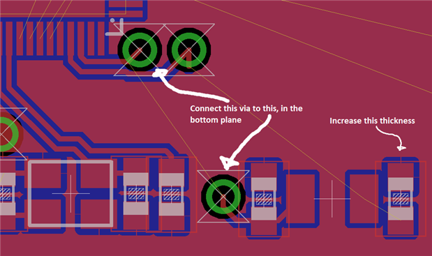
1) how do i connect these two segments? (see pic) The vias have the same name as the net. but when i try to use the routing-tool in the bottom plane, it automatically pops back up to the top plane..
2) How to i increase the thickness of the "legs" that connect the smd solder pads, to the rest of the ground-plane? (also see pic)