element14 Community
element14 Community
    Register Log In
  • Site
  • Search
  • Log In Register
  • Community Hub
    Community Hub
    • What's New on element14
    • Feedback and Support
    • Benefits of Membership
    • Personal Blogs
    • Members Area
    • Achievement Levels
  • Learn
    Learn
    • Ask an Expert
    • eBooks
    • element14 presents
    • Learning Center
    • Tech Spotlight
    • STEM Academy
    • Webinars, Training and Events
    • Learning Groups
  • Technologies
    Technologies
    • 3D Printing
    • FPGA
    • Industrial Automation
    • Internet of Things
    • Power & Energy
    • Sensors
    • Technology Groups
  • Challenges & Projects
    Challenges & Projects
    • Design Challenges
    • element14 presents Projects
    • Project14
    • Arduino Projects
    • Raspberry Pi Projects
    • Project Groups
  • Products
    Products
    • Arduino
    • Avnet & Tria Boards Community
    • Dev Tools
    • Manufacturers
    • Multicomp Pro
    • Product Groups
    • Raspberry Pi
    • RoadTests & Reviews
  • About Us
  • Store
    Store
    • Visit Your Store
    • Choose another store...
      • Europe
      •  Austria (German)
      •  Belgium (Dutch, French)
      •  Bulgaria (Bulgarian)
      •  Czech Republic (Czech)
      •  Denmark (Danish)
      •  Estonia (Estonian)
      •  Finland (Finnish)
      •  France (French)
      •  Germany (German)
      •  Hungary (Hungarian)
      •  Ireland
      •  Israel
      •  Italy (Italian)
      •  Latvia (Latvian)
      •  
      •  Lithuania (Lithuanian)
      •  Netherlands (Dutch)
      •  Norway (Norwegian)
      •  Poland (Polish)
      •  Portugal (Portuguese)
      •  Romania (Romanian)
      •  Russia (Russian)
      •  Slovakia (Slovak)
      •  Slovenia (Slovenian)
      •  Spain (Spanish)
      •  Sweden (Swedish)
      •  Switzerland(German, French)
      •  Turkey (Turkish)
      •  United Kingdom
      • Asia Pacific
      •  Australia
      •  China
      •  Hong Kong
      •  India
      • Japan
      •  Korea (Korean)
      •  Malaysia
      •  New Zealand
      •  Philippines
      •  Singapore
      •  Taiwan
      •  Thailand (Thai)
      • Vietnam
      • Americas
      •  Brazil (Portuguese)
      •  Canada
      •  Mexico (Spanish)
      •  United States
      Can't find the country/region you're looking for? Visit our export site or find a local distributor.
  • Translate
  • Profile
  • Settings
Autodesk EAGLE
  • Products
  • More
Autodesk EAGLE
EAGLE User Support (English) Questions on Eagle before sending a board off for production.
  • Blog
  • Forum
  • Documents
  • Events
  • Polls
  • Files
  • Members
  • Mentions
  • Sub-Groups
  • Tags
  • More
  • Cancel
  • New
Join Autodesk EAGLE to participate - click to join for free!
Actions
  • Share
  • More
  • Cancel
Forum Thread Details
  • State Not Answered
  • Replies 5 replies
  • Subscribers 181 subscribers
  • Views 494 views
  • Users 0 members are here
Related

Questions on Eagle before sending a board off for production.

Former Member
Former Member over 11 years ago

Hi Jorge, et. al.


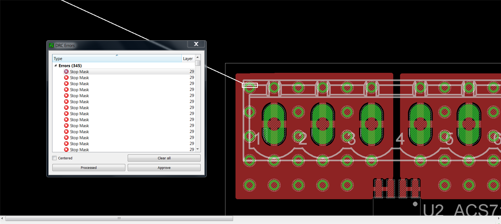
I have produced a PCB and have sent it for check at a board house and they said all is ok. Before committing I wanted to ensure success. Eagle reports 345 errors that are all in TStop layer. The solder mask crosses the silkscreen in many places, however, there is not much I can do about this, it is a tight layout. I have seen some videos on Eagle by Jeremy Blum where he states that most board houses will clean these up and to not worry about those errors.


Should I be concerned or not? I have limited experience and don't want to wait a month to receive defective boards! Your collective thoughts are appreciated in advance.


Below is an example:

image

  • Sign in to reply
  • Cancel
Parents
  • RayA
    0 RayA over 11 years ago

    I'm not an expert, but here's my take on it.


    1) The easy way would be to ask the board house to "clip" the silkscreen. Then they will automatically delete any portion of the silkscreen that interferes with exposed copper or open soldermask areas. In this case you can just "accept" the DRC errors.


    2) The better, but more time consuming way would be to delete the offending silkscreen areas manually, yourself. From the image that you included, it looks like you might need to open the library and edit the component. The "tPlace" layer can have silkscreen that DOES NOT cover up copper. This is what will print on the board. And the "tDocu" layer can have the complete silkscreen image. This is what you can print out on paper for the assembly drawing.


    Good luck.

    • Cancel
    • Vote Up 0 Vote Down
    • Sign in to reply
    • Verify Answer
    • Cancel
  • autodeskguest
    0 autodeskguest over 11 years ago in reply to RayA

    On 21/10/14 01:49, RayA wrote:

    2) The better, but more time consuming way would be to delete the

    offending silkscreen areas manually, yourself. From the image that you

    included, it looks like you might need to open the library and edit the

    component. The "tPlace" layer can have silkscreen that DOES NOT cover up

    copper. This is what will print on the board. And the "tDocu" layer can

    have the complete silkscreen image. This is what you can print out on

    paper for the assembly drawing.


    While that's a good principle, and I would certainly encourage everyone

    to design their libraries such that nothing on tPlace overlaps any pads,

    once you get to the final board layout there are likely to be at least a

    few vias that sit under the component outline sections on the xPlace

    layers. This can't be fixed in the library in any meaningful manner.


    Most board houses will clip the silkscreen.


    On one occasion, though, I had a batch of boards where they had

    erroneously clipped the top silkscreen using the bottom mask, resulting

    in a couple of fragments printed onto copper. The boards all worked fine

    anyway, although that's more by luck than judgement.


    Cheers,

    Rob


    • Cancel
    • Vote Up 0 Vote Down
    • Sign in to reply
    • Verify Answer
    • Cancel
Reply
  • autodeskguest
    0 autodeskguest over 11 years ago in reply to RayA

    On 21/10/14 01:49, RayA wrote:

    2) The better, but more time consuming way would be to delete the

    offending silkscreen areas manually, yourself. From the image that you

    included, it looks like you might need to open the library and edit the

    component. The "tPlace" layer can have silkscreen that DOES NOT cover up

    copper. This is what will print on the board. And the "tDocu" layer can

    have the complete silkscreen image. This is what you can print out on

    paper for the assembly drawing.


    While that's a good principle, and I would certainly encourage everyone

    to design their libraries such that nothing on tPlace overlaps any pads,

    once you get to the final board layout there are likely to be at least a

    few vias that sit under the component outline sections on the xPlace

    layers. This can't be fixed in the library in any meaningful manner.


    Most board houses will clip the silkscreen.


    On one occasion, though, I had a batch of boards where they had

    erroneously clipped the top silkscreen using the bottom mask, resulting

    in a couple of fragments printed onto copper. The boards all worked fine

    anyway, although that's more by luck than judgement.


    Cheers,

    Rob


    • Cancel
    • Vote Up 0 Vote Down
    • Sign in to reply
    • Verify Answer
    • Cancel
Children
No Data
element14 Community

element14 is the first online community specifically for engineers. Connect with your peers and get expert answers to your questions.

  • Members
  • Learn
  • Technologies
  • Challenges & Projects
  • Products
  • Store
  • About Us
  • Feedback & Support
  • FAQs
  • Terms of Use
  • Privacy Policy
  • Legal and Copyright Notices
  • Sitemap
  • Cookies

An Avnet Company © 2026 Premier Farnell Limited. All Rights Reserved.

Premier Farnell Ltd, registered in England and Wales (no 00876412), registered office: Farnell House, Forge Lane, Leeds LS12 2NE.

ICP 备案号 10220084.

Follow element14

  • X
  • Facebook
  • linkedin
  • YouTube