element14 Community
element14 Community
    Register Log In
  • Site
  • Search
  • Log In Register
  • Community Hub
    Community Hub
    • What's New on element14
    • Feedback and Support
    • Benefits of Membership
    • Personal Blogs
    • Members Area
    • Achievement Levels
  • Learn
    Learn
    • Ask an Expert
    • eBooks
    • element14 presents
    • Learning Center
    • Tech Spotlight
    • STEM Academy
    • Webinars, Training and Events
    • Learning Groups
  • Technologies
    Technologies
    • 3D Printing
    • FPGA
    • Industrial Automation
    • Internet of Things
    • Power & Energy
    • Sensors
    • Technology Groups
  • Challenges & Projects
    Challenges & Projects
    • Design Challenges
    • element14 presents Projects
    • Project14
    • Arduino Projects
    • Raspberry Pi Projects
    • Project Groups
  • Products
    Products
    • Arduino
    • Avnet & Tria Boards Community
    • Dev Tools
    • Manufacturers
    • Multicomp Pro
    • Product Groups
    • Raspberry Pi
    • RoadTests & Reviews
  • About Us
  • Store
    Store
    • Visit Your Store
    • Choose another store...
      • Europe
      •  Austria (German)
      •  Belgium (Dutch, French)
      •  Bulgaria (Bulgarian)
      •  Czech Republic (Czech)
      •  Denmark (Danish)
      •  Estonia (Estonian)
      •  Finland (Finnish)
      •  France (French)
      •  Germany (German)
      •  Hungary (Hungarian)
      •  Ireland
      •  Israel
      •  Italy (Italian)
      •  Latvia (Latvian)
      •  
      •  Lithuania (Lithuanian)
      •  Netherlands (Dutch)
      •  Norway (Norwegian)
      •  Poland (Polish)
      •  Portugal (Portuguese)
      •  Romania (Romanian)
      •  Russia (Russian)
      •  Slovakia (Slovak)
      •  Slovenia (Slovenian)
      •  Spain (Spanish)
      •  Sweden (Swedish)
      •  Switzerland(German, French)
      •  Turkey (Turkish)
      •  United Kingdom
      • Asia Pacific
      •  Australia
      •  China
      •  Hong Kong
      •  India
      • Japan
      •  Korea (Korean)
      •  Malaysia
      •  New Zealand
      •  Philippines
      •  Singapore
      •  Taiwan
      •  Thailand (Thai)
      • Vietnam
      • Americas
      •  Brazil (Portuguese)
      •  Canada
      •  Mexico (Spanish)
      •  United States
      Can't find the country/region you're looking for? Visit our export site or find a local distributor.
  • Translate
  • Profile
  • Settings
Autodesk EAGLE
  • Products
  • More
Autodesk EAGLE
EAGLE User Support (English) Using Eagle 7.2.0 schematic modules (hobbyist version) ... net names in module, are different from net names on a board?
  • Blog
  • Forum
  • Documents
  • Events
  • Polls
  • Files
  • Members
  • Mentions
  • Sub-Groups
  • Tags
  • More
  • Cancel
  • New
Join Autodesk EAGLE to participate - click to join for free!
Actions
  • Share
  • More
  • Cancel
Forum Thread Details
  • State Not Answered
  • Replies 1 reply
  • Subscribers 178 subscribers
  • Views 488 views
  • Users 0 members are here
  • board
  • eagle
  • name
  • net
  • editor
  • bug
  • schematic
  • polygon
  • module
Related

Using Eagle 7.2.0 schematic modules (hobbyist version) ... net names in module, are different from net names on a board?

Former Member
Former Member over 10 years ago

From a current project Version 7.2.0, Eagle Hobbyist.


In schematic module (say "AB-CDEF-1") net name is "SW1". This is is visible and can be manipulated routed, changed, etc. as normal. in a PCB layout. It is always showing up as AB-CDEF-1:SW1


I want to add in a extra polygon and VIAS on the board (power plane) to this net. What do I name it?


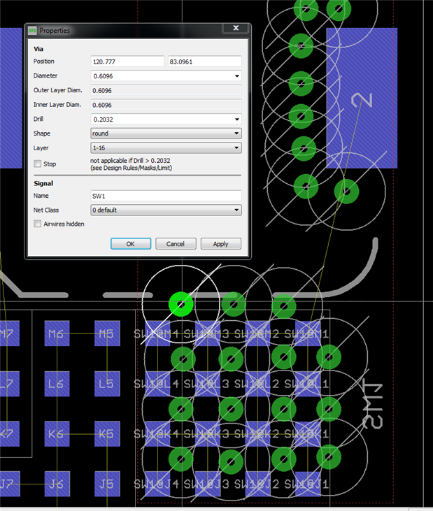
I named it "SW1", and the result is nada.


I name is "AB-CDEF-1:SW1" and the result is violation of naming protocols, as ':' is not permitted.


I edited the XML file of the pcb board file directly and it failed to load, saying I changed its tags...


So what do I do with the two unconnected nets? Where do I put a VIA on a PCB that is connected to a network wire that is in the module ?


<signal name="AB-CDEF-1:SW1">

<polygon width="0" layer="1">

<vertex x="119.678" y="93.154"/>

<vertex x="125.456" y="93.154"/>

<vertex x="126.1592" y="92.019"/>

<vertex x="126.1592" y="78.058"/>

<vertex x="119.674" y="78.058"/>

</polygon>

<via x="123.3805" y="81.7626" extent="1-16" drill="0.2032" diameter="0.6096"/>

<via x="122.047" y="81.6991" extent="1-16" drill="0.2032" diameter="0.6096"/>

<via x="120.8405" y="81.6991" extent="1-16" drill="0.2032" diameter="0.6096"/>

<via x="120.777" y="80.4291" extent="1-16" drill="0.2032" diameter="0.6096"/>

<via x="122.047" y="80.4291" extent="1-16" drill="0.2032" diameter="0.6096"/>

<via x="123.3805" y="80.4291" extent="1-16" drill="0.2032" diameter="0.6096"/>

<via x="123.3805" y="79.1591" extent="1-16" drill="0.2032" diameter="0.6096"/>

<via x="122.047" y="79.0956" extent="1-16" drill="0.2032" diameter="0.6096"/>

<via x="120.777" y="79.1591" extent="1-16" drill="0.2032" diameter="0.6096"/>

<via x="123.3805" y="83.0326" extent="1-16" drill="0.2032" diameter="0.6096"/>

<via x="122.1105" y="83.0961" extent="1-16" drill="0.2032" diameter="0.6096"/>

<via x="120.777" y="83.0961" extent="1-16" drill="0.2032" diameter="0.6096"/>

<via x="124.7775" y="90.5891" extent="1-16" drill="0.2032" diameter="0.6096"/>

<via x="123.952" y="90.5891" extent="1-16" drill="0.2032" diameter="0.6096"/>

<via x="123.825" y="89.6366" extent="1-16" drill="0.2032" diameter="0.6096"/>

<via x="123.825" y="88.6841" extent="1-16" drill="0.2032" diameter="0.6096"/>

<via x="123.825" y="87.8586" extent="1-16" drill="0.2032" diameter="0.6096"/>

<via x="123.8885" y="87.0331" extent="1-16" drill="0.2032" diameter="0.6096"/>

<via x="123.952" y="86.0806" extent="1-16" drill="0.2032" diameter="0.6096"/>

<via x="124.968" y="85.9536" extent="1-16" drill="0.2032" diameter="0.6096"/>

<via x="124.5235" y="81.7626" extent="1-16" drill="0.2032" diameter="0.6096"/>

<via x="124.5235" y="80.4291" extent="1-16" drill="0.2032" diameter="0.6096"/>

<via x="124.5235" y="79.2226" extent="1-16" drill="0.2032" diameter="0.6096"/>

</signal>

Attachments:
image
  • Sign in to reply
  • Cancel
  • Former Member
    0 Former Member over 10 years ago

    here is a better picture / explanation: Wire "SW1" is Connected to PIN #2 of a device and multiple pins of power regulator, as shown (inverted view due to components on the other side of the PCB). I needed the VIAS to be the same net name as that wire.


    SW1 is the original wire, in the module. image

    • Cancel
    • Vote Up 0 Vote Down
    • Sign in to reply
    • Verify Answer
    • Cancel
element14 Community

element14 is the first online community specifically for engineers. Connect with your peers and get expert answers to your questions.

  • Members
  • Learn
  • Technologies
  • Challenges & Projects
  • Products
  • Store
  • About Us
  • Feedback & Support
  • FAQs
  • Terms of Use
  • Privacy Policy
  • Legal and Copyright Notices
  • Sitemap
  • Cookies

An Avnet Company © 2025 Premier Farnell Limited. All Rights Reserved.

Premier Farnell Ltd, registered in England and Wales (no 00876412), registered office: Farnell House, Forge Lane, Leeds LS12 2NE.

ICP 备案号 10220084.

Follow element14

  • X
  • Facebook
  • linkedin
  • YouTube