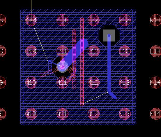
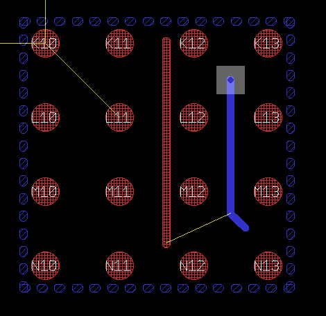
I have a .BRD with named wires and polygons, but when I go to RIPUP; it misses ripping up one of the wires, and when I RIPUP @;, it rips up the fillings, but not the wires/contours. Am I misinterpreting what the command line is to do when typed or in a .SCR? I need the functionality working in a ULP whose purpose is to partially rebuild the wires and polygons on a board.after an errant ULP trashed it. I did see something out here regarding problems with RIPUP in 7.2, so I went to 7.3 to see if it was fixed.