element14 Community
element14 Community
    Register Log In
  • Site
  • Search
  • Log In Register
  • About Us
  • Community Hub
    Community Hub
    • What's New on element14
    • Feedback and Support
    • Benefits of Membership
    • Personal Blogs
    • Members Area
    • Achievement Levels
  • Learn
    Learn
    • Ask an Expert
    • eBooks
    • element14 presents
    • Learning Center
    • Tech Spotlight
    • STEM Academy
    • Webinars, Training and Events
    • Learning Groups
  • Technologies
    Technologies
    • 3D Printing
    • FPGA
    • Industrial Automation
    • Internet of Things
    • Power & Energy
    • Sensors
    • Technology Groups
  • Challenges & Projects
    Challenges & Projects
    • Design Challenges
    • element14 presents Projects
    • Project14
    • Arduino Projects
    • Raspberry Pi Projects
    • Project Groups
  • Products
    Products
    • Arduino
    • Avnet Boards Community
    • Dev Tools
    • Manufacturers
    • Multicomp Pro
    • Product Groups
    • Raspberry Pi
    • RoadTests & Reviews
  • Store
    Store
    • Visit Your Store
    • Choose another store...
      • Europe
      •  Austria (German)
      •  Belgium (Dutch, French)
      •  Bulgaria (Bulgarian)
      •  Czech Republic (Czech)
      •  Denmark (Danish)
      •  Estonia (Estonian)
      •  Finland (Finnish)
      •  France (French)
      •  Germany (German)
      •  Hungary (Hungarian)
      •  Ireland
      •  Israel
      •  Italy (Italian)
      •  Latvia (Latvian)
      •  
      •  Lithuania (Lithuanian)
      •  Netherlands (Dutch)
      •  Norway (Norwegian)
      •  Poland (Polish)
      •  Portugal (Portuguese)
      •  Romania (Romanian)
      •  Russia (Russian)
      •  Slovakia (Slovak)
      •  Slovenia (Slovenian)
      •  Spain (Spanish)
      •  Sweden (Swedish)
      •  Switzerland(German, French)
      •  Turkey (Turkish)
      •  United Kingdom
      • Asia Pacific
      •  Australia
      •  China
      •  Hong Kong
      •  India
      •  Korea (Korean)
      •  Malaysia
      •  New Zealand
      •  Philippines
      •  Singapore
      •  Taiwan
      •  Thailand (Thai)
      • Americas
      •  Brazil (Portuguese)
      •  Canada
      •  Mexico (Spanish)
      •  United States
      Can't find the country/region you're looking for? Visit our export site or find a local distributor.
  • Translate
  • Profile
  • Settings
Autodesk EAGLE
  • Products
  • More
Autodesk EAGLE
EAGLE User Support (English) Net class specifications and name of some components
  • Blog
  • Forum
  • Documents
  • Events
  • Polls
  • Files
  • Members
  • Mentions
  • Sub-Groups
  • Tags
  • More
  • Cancel
  • New
Join Autodesk EAGLE to participate - click to join for free!
Actions
  • Share
  • More
  • Cancel
Forum Thread Details
  • Replies 9 replies
  • Subscribers 175 subscribers
  • Views 652 views
  • Users 0 members are here
  • netclass
  • components.
Related

Net class specifications and name of some components

Former Member
Former Member over 9 years ago

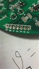
Hello guys first of all i want to point that i dont have any experience about eagle and i am trying to design a pcb. It will be a commercial product so it needs to be perfect. I have finished my schematic design. There is no problem about that however i have some troubles in board part as you can guess. Firstly net class specifications i made, width 12mil,drill 20mil and clearance 12mil and i got 730 errors about them from drc checking. So what are wrongs with these numbers. What are the things i should be worry about when i am arranging them. In which case i should create more than one net class why ? Also   i want to make these holes in pcb. Because i just want to put 433 mhz rf module on it. So what should i put in the schematic to use them. These are not headers right ? Also i assumed that they are not just holes which you can make from board design or are they ? image

  • Sign in to reply
  • Cancel
Parents
  • autodeskguest
    autodeskguest over 9 years ago

    On 07/31/2016 09:43 AM, Zeki Caner Adıyaman wrote:

    i got 730 errors about them from drc checking.

    You have to select each one to see what the issue is.

    Traces crossing traces (shorts) would give many errors.

    Just work on the list a little first.

    Paul R


    • Cancel
    • Vote Up 0 Vote Down
    • Sign in to reply
    • Cancel
  • Former Member
    Former Member over 9 years ago in reply to autodeskguest

    I am using arduino nano and all these errors come from arduino part of the pcb

    • Cancel
    • Vote Up 0 Vote Down
    • Sign in to reply
    • Cancel
  • autodeskguest
    autodeskguest over 9 years ago in reply to Former Member

    On 07/31/2016 10:26 AM, Zeki Caner Adıyaman wrote:

    I am using arduino nano and all these errors come from arduino part of the pcb


    --

    To view any images and attachments in this post, visit:

    https://www.element14.com/community/message/202705


    Other threads had issues related to putting the layout and schematic of

    a plug in module into the PCB assembly. If you are mounting surface

    mount parts with fine pitch the part won't pass 12mil clearance and

    trace width.

    Paul


    • Cancel
    • Vote Up 0 Vote Down
    • Sign in to reply
    • Cancel
  • Former Member
    Former Member over 9 years ago in reply to autodeskguest

    What are the bad effects of decreasing clearance,width or drill ? For example i heard if there is high voltage on the wire clearance should be bigger . Is there any tip like that i must know

    • Cancel
    • Vote Up 0 Vote Down
    • Sign in to reply
    • Cancel
  • autodeskguest
    autodeskguest over 9 years ago in reply to Former Member

    On 07/31/2016 11:54 AM, Zeki Caner Adıyaman wrote:

    What are the bad effects of decreasing clearance,width or drill ? For example i heard if there is high voltage on the wire clearance should be bigger . Is there any tip like that i must know


    --

    To view any images and attachments in this post, visit:

    https://www.element14.com/community/message/202796


    Most pcb houses do 8mil trace and clearance for no extra charge.

    At lower voltages the pcb manufacture you pick will set the limits. At

    higher voltages clearances depend on the regulatory rules in place where

    you are selling.


    The first few hits from duckduckgo.com


    http://www.smps.us/pcbtracespacing.html

    http://www.electronics-project-design.com/PCB-Design.html


    Paul


    • Cancel
    • Vote Up 0 Vote Down
    • Sign in to reply
    • Cancel
  • omega-5
    omega-5 over 9 years ago in reply to Former Member

    Am 31.07.2016 um 16:26 schrieb Zeki Caner Adıyaman:

    I am using arduino nano and all these errors come from arduino part of the pcb


    --

    To view any images and attachments in this post, visit:

    https://www.element14.com/community/message/202705


    Which library do you use? Because there are libraries out there

    with errors in the layer assignment.


    Freundliche Grüße / Kind regards

    Friedrich

    -


    ... benutzen Sie nntp://news.cadsoft.de und einen

    funktionierenden News-Reader wie Thunderbird!

    ... use NNTP://news.cadsoft.de and a

    functional news reader like Thunderbird!


    • Cancel
    • Vote Up 0 Vote Down
    • Sign in to reply
    • Cancel
Reply
  • omega-5
    omega-5 over 9 years ago in reply to Former Member

    Am 31.07.2016 um 16:26 schrieb Zeki Caner Adıyaman:

    I am using arduino nano and all these errors come from arduino part of the pcb


    --

    To view any images and attachments in this post, visit:

    https://www.element14.com/community/message/202705


    Which library do you use? Because there are libraries out there

    with errors in the layer assignment.


    Freundliche Grüße / Kind regards

    Friedrich

    -


    ... benutzen Sie nntp://news.cadsoft.de und einen

    funktionierenden News-Reader wie Thunderbird!

    ... use NNTP://news.cadsoft.de and a

    functional news reader like Thunderbird!


    • Cancel
    • Vote Up 0 Vote Down
    • Sign in to reply
    • Cancel
Children
No Data
element14 Community

element14 is the first online community specifically for engineers. Connect with your peers and get expert answers to your questions.

  • Members
  • Learn
  • Technologies
  • Challenges & Projects
  • Products
  • Store
  • About Us
  • Feedback & Support
  • FAQs
  • Terms of Use
  • Privacy Policy
  • Legal and Copyright Notices
  • Sitemap
  • Cookies

An Avnet Company © 2025 Premier Farnell Limited. All Rights Reserved.

Premier Farnell Ltd, registered in England and Wales (no 00876412), registered office: Farnell House, Forge Lane, Leeds LS12 2NE.

ICP 备案号 10220084.

Follow element14

  • X
  • Facebook
  • linkedin
  • YouTube