Good Morning,
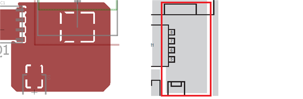
I have a 2 Layers PCB and I have to design a polygon (as the datasheet suggest) which surrounds three devices pad as you can see in the attached file (red rectangle).
I wonder if I can set on the thermals without losing the benefits of polygon (as you can see the attached file ).
Setting on the thermals will give me an help for hand soldering but my fear is that I should lose the benefits of the polygon.
Sorry for this dummy question but I'm not an HW expert.
Hope you can help
Thanks a lotù
Nico