


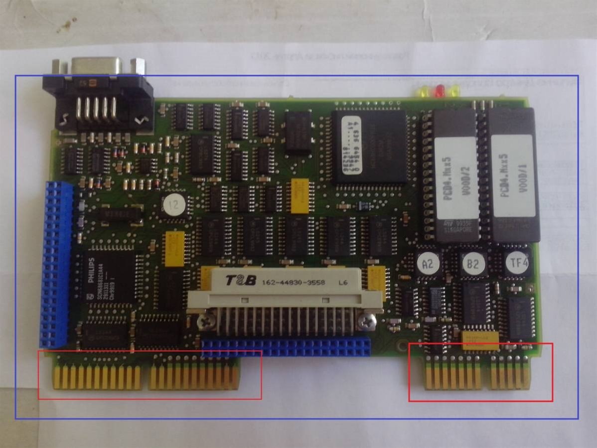
Hello everybody. How to make a similar plug on the board circled in red in Eagle cad? And how to make such a board size circled in blue. Thank you.

Hello everybody. How to make a similar plug on the board circled in red in Eagle cad? And how to make such a board size circled in blue. Thank you.


