element14 Community
element14 Community
    Register Log In
  • Site
  • Search
  • Log In Register
  • Community Hub
    Community Hub
    • What's New on element14
    • Feedback and Support
    • Benefits of Membership
    • Personal Blogs
    • Members Area
    • Achievement Levels
  • Learn
    Learn
    • Ask an Expert
    • eBooks
    • element14 presents
    • Learning Center
    • Tech Spotlight
    • STEM Academy
    • Webinars, Training and Events
    • Learning Groups
  • Technologies
    Technologies
    • 3D Printing
    • FPGA
    • Industrial Automation
    • Internet of Things
    • Power & Energy
    • Sensors
    • Technology Groups
  • Challenges & Projects
    Challenges & Projects
    • Design Challenges
    • element14 presents Projects
    • Project14
    • Arduino Projects
    • Raspberry Pi Projects
    • Project Groups
  • Products
    Products
    • Arduino
    • Avnet & Tria Boards Community
    • Dev Tools
    • Manufacturers
    • Multicomp Pro
    • Product Groups
    • Raspberry Pi
    • RoadTests & Reviews
  • About Us
    About the element14 Community
  • Store
    Store
    • Visit Your Store
    • Choose another store...
      • Europe
      •  Austria (German)
      •  Belgium (Dutch, French)
      •  Bulgaria (Bulgarian)
      •  Czech Republic (Czech)
      •  Denmark (Danish)
      •  Estonia (Estonian)
      •  Finland (Finnish)
      •  France (French)
      •  Germany (German)
      •  Hungary (Hungarian)
      •  Ireland
      •  Israel
      •  Italy (Italian)
      •  Latvia (Latvian)
      •  
      •  Lithuania (Lithuanian)
      •  Netherlands (Dutch)
      •  Norway (Norwegian)
      •  Poland (Polish)
      •  Portugal (Portuguese)
      •  Romania (Romanian)
      •  Russia (Russian)
      •  Slovakia (Slovak)
      •  Slovenia (Slovenian)
      •  Spain (Spanish)
      •  Sweden (Swedish)
      •  Switzerland(German, French)
      •  Turkey (Turkish)
      •  United Kingdom
      • Asia Pacific
      •  Australia
      •  China
      •  Hong Kong
      •  India
      •  Japan
      •  Korea (Korean)
      •  Malaysia
      •  New Zealand
      •  Philippines
      •  Singapore
      •  Taiwan
      •  Thailand (Thai)
      •  Vietnam
      • Americas
      •  Brazil (Portuguese)
      •  Canada
      •  Mexico (Spanish)
      •  United States
      Can't find the country/region you're looking for? Visit our export site or find a local distributor.
  • Translate
  • Profile
  • Settings
Autodesk EAGLE
  • Products
  • More
Autodesk EAGLE
EAGLE User Support (English) Connector SL
  • Blog
  • Forum
  • Documents
  • Events
  • Polls
  • Files
  • Members
  • Mentions
  • Sub-Groups
  • Tags
  • More
  • Cancel
  • New
Join Autodesk EAGLE to participate - click to join for free!
Actions
  • Share
  • More
  • Cancel
Forum Thread Details
  • Replies 7 replies
  • Subscribers 189 subscribers
  • Views 1480 views
  • Users 0 members are here
Related

Connector SL

dmitrius
dmitrius over 9 years ago

Hello everybody. How to make a similar plug on the board circled in red in Eagle cad? And how to make such a board size circled in blue. Thank you.
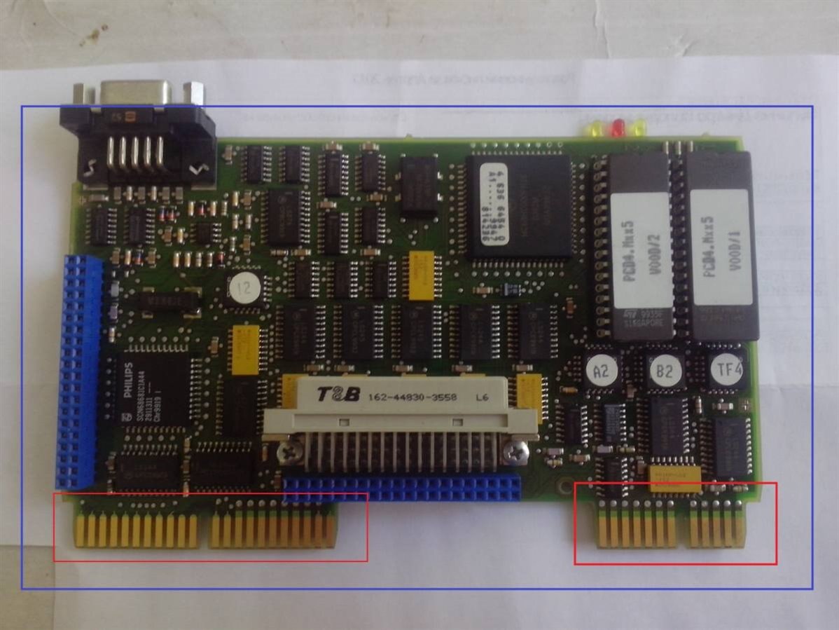
image

image

  • Sign in to reply
  • Cancel
Parents
  • autodeskguest
    autodeskguest over 9 years ago

    On 06.06.2017 10:55, Dmitriy Vladimirovich wrote:

    Hello everybody. How to make a similar plug on the board circled in red in Eagle cad? And how to make such a board size circled in blue. Thank you.


    There are some issues you also need to take care of, and Eagle is not

    helping much. They need to be specified to the manufacturer next to the

    gerbers.


    1-Make sure the PCB thickness is matching your socket (Yea, I've managed

    to mess up this once!). If it's 1.6mm, you have a great chance of

    accidentially getting it right.


    2-The card edge needs beveling (v'shape) to be gentle to the receptor.

    See datasheet of the receptor for recommendations.


    3-The contacts need special coating to prevent oxidation. Normally this

    is done in production by shorting all the pins before final cutout,

    applying a voltage to them all while the edge of the pcb is dipped into

    some chemical for coating deposit, then the shorts are cut out and

    beveling applied. You can often see the thin tracks that used to short

    circuit all the pins as leftover on the wider pads.


    Also see http://www.eurocircuits.com/blog/gold-plating-for-edge-connectors/


    • Cancel
    • Vote Up +3 Vote Down
    • Sign in to reply
    • Cancel
Reply
  • autodeskguest
    autodeskguest over 9 years ago

    On 06.06.2017 10:55, Dmitriy Vladimirovich wrote:

    Hello everybody. How to make a similar plug on the board circled in red in Eagle cad? And how to make such a board size circled in blue. Thank you.


    There are some issues you also need to take care of, and Eagle is not

    helping much. They need to be specified to the manufacturer next to the

    gerbers.


    1-Make sure the PCB thickness is matching your socket (Yea, I've managed

    to mess up this once!). If it's 1.6mm, you have a great chance of

    accidentially getting it right.


    2-The card edge needs beveling (v'shape) to be gentle to the receptor.

    See datasheet of the receptor for recommendations.


    3-The contacts need special coating to prevent oxidation. Normally this

    is done in production by shorting all the pins before final cutout,

    applying a voltage to them all while the edge of the pcb is dipped into

    some chemical for coating deposit, then the shorts are cut out and

    beveling applied. You can often see the thin tracks that used to short

    circuit all the pins as leftover on the wider pads.


    Also see http://www.eurocircuits.com/blog/gold-plating-for-edge-connectors/


    • Cancel
    • Vote Up +3 Vote Down
    • Sign in to reply
    • Cancel
Children
  • rachaelp
    rachaelp over 9 years ago in reply to autodeskguest

    Hi Morten,

    There are some issues you also need to take care of, and Eagle is not

    helping much. They need to be specified to the manufacturer next to the

    gerbers.


    You are right, special care needs to be taken to ensure that the board manufacturer sees and acts upon the additional information. Is there a standard way other tools do this that you know of? I've only ever seen notes added to drawings which are printed and supplied as part of the gerber set... But I have seen those completely ignored previously so you have to work especially hard to ensure that your board house really has paid attention to any additional information supplied.

    1-Make sure the PCB thickness is matching your socket (Yea, I've managed

    to mess up this once!). If it's 1.6mm, you have a great chance of

    accidentially getting it right.

    That's a very good point, I guess lots of people learn that lesson the hard way.... In fact I will be designing a board with a card edge soon so I will make a note of that now so I don't forget and have a stupid fail on the first prototype! image

    2-The card edge needs beveling (v'shape) to be gentle to the receptor.

    See datasheet of the receptor for recommendations.


    3-The contacts need special coating to prevent oxidation. Normally this

    is done in production by shorting all the pins before final cutout,

    applying a voltage to them all while the edge of the pcb is dipped into

    some chemical for coating deposit, then the shorts are cut out and

    beveling applied. You can often see the thin tracks that used to short

    circuit all the pins as leftover on the wider pads.

    These are the two things I mentioned in my post, but I probably wasn't clear enough about the gold plating. So, the process you refer to is actually to produce a harder gold plating for the connector fingers rather than the softer plating you get when you have a typical gold finished board. It's not about a surface to protect from oxidation, its so it's mechanically strong enough surface that it can withstand insertion into the edge connector socket without damaging the surface. I didn't actually know how it was done and that extra shorting traces were required which were then removed as part of the bevelling. Very useful info, thanks image

    Also see http://www.eurocircuits.com/blog/gold-plating-for-edge-connectors/

    Ahhh, Eurocircuits, my go to board house for prototype boards. I've bookmarked that link for my upcoming project. Thanks image


    Best Regards,


    Rachael

    • Cancel
    • Vote Up +2 Vote Down
    • Sign in to reply
    • Cancel
element14 Community

element14 is the first online community specifically for engineers. Connect with your peers and get expert answers to your questions.

  • Members
  • Learn
  • Technologies
  • Challenges & Projects
  • Products
  • Store
  • About Us
  • Feedback & Support
  • FAQs
  • Terms of Use
  • Privacy Policy
  • Legal and Copyright Notices
  • Sitemap
  • Cookies

An Avnet Company © 2026 Premier Farnell Limited. All Rights Reserved.

Premier Farnell Ltd, registered in England and Wales (no 00876412), registered office: Farnell House, Forge Lane, Leeds LS12 2NE.

Follow element14

  • X
  • Facebook
  • linkedin
  • YouTube