Hello everybody,
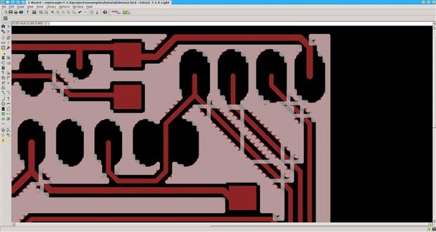
I'm wondering if following is possible. I need to have a ratsnets being made based on top layer, but the polygon itself needs to be stored in a different layer. I need to automate process with cam and I need to have it stored under different layer to apply different settings to the job. But the ratsnets needs to be decided on the top layer.
Thanks in advance for any hints or ideas.
PS: if it's possible in any specific version I don't mind upgrading/downgrading.