element14 Community
element14 Community
    Register Log In
  • Site
  • Search
  • Log In Register
  • Community Hub
    Community Hub
    • What's New on element14
    • Feedback and Support
    • Benefits of Membership
    • Personal Blogs
    • Members Area
    • Achievement Levels
  • Learn
    Learn
    • Ask an Expert
    • eBooks
    • element14 presents
    • Learning Center
    • Tech Spotlight
    • STEM Academy
    • Webinars, Training and Events
    • Learning Groups
  • Technologies
    Technologies
    • 3D Printing
    • FPGA
    • Industrial Automation
    • Internet of Things
    • Power & Energy
    • Sensors
    • Technology Groups
  • Challenges & Projects
    Challenges & Projects
    • Design Challenges
    • element14 presents Projects
    • Project14
    • Arduino Projects
    • Raspberry Pi Projects
    • Project Groups
  • Products
    Products
    • Arduino
    • Avnet & Tria Boards Community
    • Dev Tools
    • Manufacturers
    • Multicomp Pro
    • Product Groups
    • Raspberry Pi
    • RoadTests & Reviews
  • About Us
    About the element14 Community
  • Store
    Store
    • Visit Your Store
    • Choose another store...
      • Europe
      •  Austria (German)
      •  Belgium (Dutch, French)
      •  Bulgaria (Bulgarian)
      •  Czech Republic (Czech)
      •  Denmark (Danish)
      •  Estonia (Estonian)
      •  Finland (Finnish)
      •  France (French)
      •  Germany (German)
      •  Hungary (Hungarian)
      •  Ireland
      •  Israel
      •  Italy (Italian)
      •  Latvia (Latvian)
      •  
      •  Lithuania (Lithuanian)
      •  Netherlands (Dutch)
      •  Norway (Norwegian)
      •  Poland (Polish)
      •  Portugal (Portuguese)
      •  Romania (Romanian)
      •  Russia (Russian)
      •  Slovakia (Slovak)
      •  Slovenia (Slovenian)
      •  Spain (Spanish)
      •  Sweden (Swedish)
      •  Switzerland(German, French)
      •  Turkey (Turkish)
      •  United Kingdom
      • Asia Pacific
      •  Australia
      •  China
      •  Hong Kong
      •  India
      •  Japan
      •  Korea (Korean)
      •  Malaysia
      •  New Zealand
      •  Philippines
      •  Singapore
      •  Taiwan
      •  Thailand (Thai)
      •  Vietnam
      • Americas
      •  Brazil (Portuguese)
      •  Canada
      •  Mexico (Spanish)
      •  United States
      Can't find the country/region you're looking for? Visit our export site or find a local distributor.
  • Translate
  • Profile
  • Settings
Autodesk EAGLE
  • Products
  • More
Autodesk EAGLE
Forum Have a question about CadSoft EAGLE?  Ask our Expert, Richard! (Archive)
  • Blog
  • Forum
  • Documents
  • Events
  • Polls
  • Files
  • Members
  • Mentions
  • Sub-Groups
  • Tags
  • More
  • Cancel
  • New
Join Autodesk EAGLE to participate - click to join for free!
Actions
  • Share
  • More
  • Cancel
Forum Thread Details
  • Replies 1129 replies
  • Subscribers 245 subscribers
  • Views 51363 views
  • Users 0 members are here
  • eagle
  • expert
  • richard_hammerl
  • cadsoft
Related

Have a question about CadSoft EAGLE?  Ask our Expert, Richard! (Archive)

nlarson
nlarson over 16 years ago

This thread is now locked - but you can still ask Richard by posting your questions here.  If you'd rather browse other member's questions you can read the CadSoft EAGLE Forums for past questions and answers. Enjoy!


Browse past Q&A help on anything technical relating to CadSoft EAGLE!


image


Richard Hammerl

Richard is an engineer with 16 years experience in EAGLE customer support and is waiting for your questions.

  • Sign in to reply
  • Cancel
  • Richard_H
    Richard_H over 15 years ago in reply to DSFe

    Hi Daniel,


    as far as I know no such package is currently available in our libraries. So you have to create it by yourself. Place 8 SMD pads and draw a polygon or place the large SMD so that it covers the drain contacts. Using a polygon will cause DRC errors in the layout. The reason is that you can't name the polygon in the package editor and assign it to a certain signal. This is not a problem at all, you can approve these error messages.


    In case you use a SMD for the big area, you should place an additional pin in the symbol. You won't have DRC errors in the layout then.


    Hope this helps.

    Regards,

    Richard

    • Cancel
    • Vote Up 0 Vote Down
    • Sign in to reply
    • Cancel
  • e14 Contributor
    e14 Contributor over 15 years ago

    Hey Richard,


    I was wondering if it is possible to add a graphics image to the Schematic section of my circuit?


    What I am wanting to do is add a captured image from my O-Scope to the schematics to show what the circuit is doing.

    How would I do this?


    Is this possible or is it going to be easier to export the schematic to pdf format and then go through and edit the pdf and add them there?


    Thank you for your time.

    • Cancel
    • Vote Up 0 Vote Down
    • Sign in to reply
    • Cancel
  • DSFe
    DSFe over 15 years ago
    Dear Richard,
     
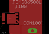
    I’m trying to use FDMS86101FDMS86101 ( farnell code 1885754 ) and I’m having difficulties drawing the component Pad.
     
    Do you know if there is already the component available in a library?
     
    In the library I’ve created the different areas with gave me errors in  the eagles DRC and more important don’t able me to generate thermal pad around. Please see attached picture. Do you have a solution for this?
     
    Danielimage
    • Cancel
    • Vote Up 0 Vote Down
    • Sign in to reply
    • Cancel
  • Richard_H
    Richard_H over 15 years ago in reply to e14 Contributor

    Hello,


    a thermal symbol looks like shown in the attached image.

    Concerning Gerber data and CAM Processor: The inner layer has to be combined with pads and vias in order to get proper Gerber data. it is treated like Top or Bottom.

    image

    Regards,

    Richard

    • Cancel
    • Vote Up 0 Vote Down
    • Sign in to reply
    • Cancel
  • e14 Contributor
    e14 Contributor over 15 years ago in reply to e14 Contributor

    Sir,


    I found out the option under 'change--> thermals--> ON'. Using this option i can see the ring formation of the filling around the respective signal vias. Are these the thermals?


    And when I'll be using the CAM Processor, doi have to select the pads and vias like how we do for the top and bottom layer or do i have to just select the signal layer as in case of the sagnal layer with a $ sign?

    • Cancel
    • Vote Up 0 Vote Down
    • Sign in to reply
    • Cancel
  • e14 Contributor
    e14 Contributor over 15 years ago in reply to Richard_H

    Hello Sir,


    It wa so kind of you to answer my query so quickly.


    Sir, I did try out the polygon method. It does work but the main point is that it does not show thermal vias for any signal, may it be GND or VCC or 5V or any other.


    My other colleages have designed a similar 4 layered board using PADS software. And the gerber viewer (we are using Gerbv) shows thermal pads for all the different types of grounds and powers that they have used, but it is not the case with Eagle..Please help me with this problem of mine..

    • Cancel
    • Vote Up 0 Vote Down
    • Sign in to reply
    • Cancel
  • Richard_H
    Richard_H over 15 years ago in reply to e14 Contributor

    Hello,


    to realize three different GND signals within one layer, you have to use polygons in one of the inner signal layers. Please don't use a Supply layer (which has the a $ character at the beginning) because such a supply layer is displayed and plotted inverted and leads exactly one signal. The signal you specify with the supply layer's name.


    So what you have to do is to use an inner layer and draw three different POLYGONs. Name the polygons the same as the signal they should belong to. And think about the polygon property "Rank" which determines the priority of the polygon.  Additional help can be found in our FAQ:

    http://www.cadsoftusa.com/training/faq/#17


    Regards,

    Richard

    • Cancel
    • Vote Up 0 Vote Down
    • Sign in to reply
    • Cancel
  • e14 Contributor
    e14 Contributor over 15 years ago

    Hello Sir,

    I am designing a 4 layered board in Eagle. My ground layer has 3 types of grounds namely GND,AGND,GND, which are supposed to be in the same layer GND.

    one  of my signal layer is $GND and so only my GND shows thermal vias on  that layer while other (AGND,GND1) show isolated rings...plz help me  with this poblem..

    • Cancel
    • Vote Up 0 Vote Down
    • Sign in to reply
    • Cancel
  • Richard_H
    Richard_H over 15 years ago in reply to e14 Contributor

    Hi,


    no I am sorry. EAGLE has no possibilities that allow setting a password to a file.


    Regards,

    Richard

    • Cancel
    • Vote Up 0 Vote Down
    • Sign in to reply
    • Cancel
  • Richard_H
    Richard_H over 15 years ago in reply to jpmerron

    Hi John,


    after specifying a netclass you have to assign the netclass to a net. This can be done for example via the properties dialog of a net. You can also use CHANGE CLASS and click onto the net you want to assign.


    Regards,

    Richard

    • Cancel
    • Vote Up 0 Vote Down
    • Sign in to reply
    • Cancel
<>
element14 Community

element14 is the first online community specifically for engineers. Connect with your peers and get expert answers to your questions.

  • Members
  • Learn
  • Technologies
  • Challenges & Projects
  • Products
  • Store
  • About Us
  • Feedback & Support
  • FAQs
  • Terms of Use
  • Privacy Policy
  • Legal and Copyright Notices
  • Sitemap
  • Cookies

An Avnet Company © 2026 Premier Farnell Limited. All Rights Reserved.

Premier Farnell Ltd, registered in England and Wales (no 00876412), registered office: Farnell House, Forge Lane, Leeds LS12 2NE.

Follow element14

  • X
  • Facebook
  • linkedin
  • YouTube