element14 Community
element14 Community
    Register Log In
  • Site
  • Search
  • Log In Register
  • Community Hub
    Community Hub
    • What's New on element14
    • Feedback and Support
    • Benefits of Membership
    • Personal Blogs
    • Members Area
    • Achievement Levels
  • Learn
    Learn
    • Ask an Expert
    • eBooks
    • element14 presents
    • Learning Center
    • Tech Spotlight
    • STEM Academy
    • Webinars, Training and Events
    • Learning Groups
  • Technologies
    Technologies
    • 3D Printing
    • FPGA
    • Industrial Automation
    • Internet of Things
    • Power & Energy
    • Sensors
    • Technology Groups
  • Challenges & Projects
    Challenges & Projects
    • Design Challenges
    • element14 presents Projects
    • Project14
    • Arduino Projects
    • Raspberry Pi Projects
    • Project Groups
  • Products
    Products
    • Arduino
    • Avnet & Tria Boards Community
    • Dev Tools
    • Manufacturers
    • Multicomp Pro
    • Product Groups
    • Raspberry Pi
    • RoadTests & Reviews
  • About Us
    About the element14 Community
  • Store
    Store
    • Visit Your Store
    • Choose another store...
      • Europe
      •  Austria (German)
      •  Belgium (Dutch, French)
      •  Bulgaria (Bulgarian)
      •  Czech Republic (Czech)
      •  Denmark (Danish)
      •  Estonia (Estonian)
      •  Finland (Finnish)
      •  France (French)
      •  Germany (German)
      •  Hungary (Hungarian)
      •  Ireland
      •  Israel
      •  Italy (Italian)
      •  Latvia (Latvian)
      •  
      •  Lithuania (Lithuanian)
      •  Netherlands (Dutch)
      •  Norway (Norwegian)
      •  Poland (Polish)
      •  Portugal (Portuguese)
      •  Romania (Romanian)
      •  Russia (Russian)
      •  Slovakia (Slovak)
      •  Slovenia (Slovenian)
      •  Spain (Spanish)
      •  Sweden (Swedish)
      •  Switzerland(German, French)
      •  Turkey (Turkish)
      •  United Kingdom
      • Asia Pacific
      •  Australia
      •  China
      •  Hong Kong
      •  India
      •  Japan
      •  Korea (Korean)
      •  Malaysia
      •  New Zealand
      •  Philippines
      •  Singapore
      •  Taiwan
      •  Thailand (Thai)
      •  Vietnam
      • Americas
      •  Brazil (Portuguese)
      •  Canada
      •  Mexico (Spanish)
      •  United States
      Can't find the country/region you're looking for? Visit our export site or find a local distributor.
  • Translate
  • Profile
  • Settings
Autodesk EAGLE
  • Products
  • More
Autodesk EAGLE
Forum Have a question about CadSoft EAGLE?  Ask our Expert, Richard! (Archive)
  • Blog
  • Forum
  • Documents
  • Events
  • Polls
  • Files
  • Members
  • Mentions
  • Sub-Groups
  • Tags
  • More
  • Cancel
  • New
Join Autodesk EAGLE to participate - click to join for free!
Actions
  • Share
  • More
  • Cancel
Forum Thread Details
  • Replies 1129 replies
  • Subscribers 245 subscribers
  • Views 51411 views
  • Users 0 members are here
  • eagle
  • expert
  • richard_hammerl
  • cadsoft
Related

Have a question about CadSoft EAGLE?  Ask our Expert, Richard! (Archive)

nlarson
nlarson over 16 years ago

This thread is now locked - but you can still ask Richard by posting your questions here.  If you'd rather browse other member's questions you can read the CadSoft EAGLE Forums for past questions and answers. Enjoy!


Browse past Q&A help on anything technical relating to CadSoft EAGLE!


image


Richard Hammerl

Richard is an engineer with 16 years experience in EAGLE customer support and is waiting for your questions.

  • Sign in to reply
  • Cancel
  • e14 Contributor
    e14 Contributor over 15 years ago

    Hi,

        I hope all of you are fine, I have to generate XY data file from the .Brd file  for SMT automated placement. So refer me one ULP. Earlier I had used "Picknplace.ulp".but i dont have it right now from where i can down load it


    Thanks in advance.

    • Cancel
    • Vote Up 0 Vote Down
    • Sign in to reply
    • Cancel
  • e14 Contributor
    e14 Contributor over 15 years ago

    I am setting up a multilayer board and I'm a bit confused.

    I would like to set up four layers.

    Top wil be signal

    Second will be signal

    Third will be power

    Fourth will be ground.


    I would like to set it up so that I can have blind vias from the top and second  layers to any of the other layers. (and each other)


    I am having trouble understanding the syntax to set up the layers and the blind and buried vias.


    Also, depending on the way I describe the layers and connections, the vias either go to the top of a layer or they seem to go through to  the other  side of the layer.   I am not sure of the significance of this.    Your help is appreciated.


    Thanks,

    Joe A.

    • Cancel
    • Vote Up 0 Vote Down
    • Sign in to reply
    • Cancel
  • e14 Contributor
    e14 Contributor over 15 years ago

    Richard,


    Does element14 have an eagle library for PIC18F*50 series microcontrollers; namely PIC18F14K50. I have a need for a component spec but can't find it in any libraries (even PIC micro). Otherwise, can you tell me where I might find one?


    Many Thanks.

    • Cancel
    • Vote Up 0 Vote Down
    • Sign in to reply
    • Cancel
  • levafreidin
    levafreidin over 15 years ago in reply to e14 Contributor

        Hello Jskene,

             For 20 pins, you can make footprint by yourself for half an hour. Pay attention: exposed pad has to be connected to ground, so it is the pin, #21. For automatic assembly, you can follow the Atmel's drawing. For manual assembly (prototyping PCB), I usually drill hole (so, it became Through Hole Pin) large enough for my soldering iron tip. I also use low temperature solder to connect it to the Ground Plane, to avoid overheating.

        For manual assembly, it is also good idea to make SMD pads a little bit longer, to make soldering easier.

        If you need real help (not advise), you can reach me by e-mail "levafreidin@yahoo.com" or phone (805)-750-0665 cell.

             Good luck!

                  Lev.

    • Cancel
    • Vote Up 0 Vote Down
    • Sign in to reply
    • Cancel
  • Richard_H
    Richard_H over 15 years ago in reply to DSFe

    Hi Daniel,


    maybe it is enough to change the width of the polygon? This affects the thermal reliefs as well. The width of the connecting wires are getting thiker with increasing the polygon's width.


    On the other hand you could draw a second polygon with the same signal name over/around the smd and change the width for it. So it only affects this restricted area.


    You could also change the Thermals parameter of the polygon. Set it off, and the SMDs will be connected without thermal reliefs.


    Hope this helps.


    Regards,

    Richard

    • Cancel
    • Vote Up 0 Vote Down
    • Sign in to reply
    • Cancel
  • DSFe
    DSFe over 15 years ago
    Dear Richard,
     
    Is there any fast way to add cooper in a SMD component to reduce thermal resistance without changing the component footprint?
     
    Thanks
    Daniel
    • Cancel
    • Vote Up 0 Vote Down
    • Sign in to reply
    • Cancel
  • e14 Contributor
    e14 Contributor over 15 years ago in reply to Richard_H

    Does anyone know where I can find an Eagle footprint for a QFN-20 3mm x 3mm? The only ones I can find are 4mm x 4mm.


    This is for an Atmel ATtiny24A-MMH


    Thanks;


    JS

    • Cancel
    • Vote Up 0 Vote Down
    • Sign in to reply
    • Cancel
  • Richard_H
    Richard_H over 15 years ago in reply to e14 Contributor

    HI,


    just saw your message here, after answering the same question in german. But here you attached a picture which could help a bit. When you use RATSNEST for calculating the polygons, are the polygons filled? Do they have the name of the signal the should belong to?

    It is difficult to give advice here, could you send me the board file via private email to supoprt@cadsoft.de.

    So I can take a look into it.


    Regards,

    Richard

    • Cancel
    • Vote Up 0 Vote Down
    • Sign in to reply
    • Cancel
  • e14 Contributor
    e14 Contributor over 15 years ago

    Hi richard,


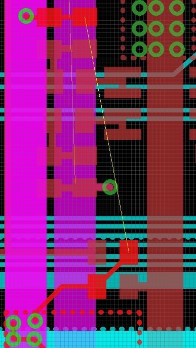
    I´ve got a hand routed layout. Though each net is physically completely connected there are still air-wires left (see attached picture). Ratsnest brings no change. Is there any solution except of routing those air-wires ? Using the Auto-Router is no option - it´s an hf-design.


    Thanks in advance


    Uwe


    image

    • Cancel
    • Vote Up 0 Vote Down
    • Sign in to reply
    • Cancel
  • Richard_H
    Richard_H over 15 years ago in reply to e14 Contributor

    Hi Arnauld,


    it is not quite correct. You have to use two coordinates: One for selecting the group and setting a reference and the second one in order to specify where to place the group.

    It can look like this:

      GROUP ALL;

      MOVE  (C>0 0)  (-7.5 -8.4);


    The first coordinate contains C> for Ctrl + right mouse click at location (0 0) for accessing the group.

    The secon is the left mous click to place the group.


    If you are working with an EAGLE version before 5, you don't need the Ctrl key. Then it would look like this:

    MOVE  (>0 0)  (-7.5 -8.4);


    Regards,

    Richard

    • Cancel
    • Vote Up 0 Vote Down
    • Sign in to reply
    • Cancel
<>
element14 Community

element14 is the first online community specifically for engineers. Connect with your peers and get expert answers to your questions.

  • Members
  • Learn
  • Technologies
  • Challenges & Projects
  • Products
  • Store
  • About Us
  • Feedback & Support
  • FAQs
  • Terms of Use
  • Privacy Policy
  • Legal and Copyright Notices
  • Sitemap
  • Cookies

An Avnet Company © 2026 Premier Farnell Limited. All Rights Reserved.

Premier Farnell Ltd, registered in England and Wales (no 00876412), registered office: Farnell House, Forge Lane, Leeds LS12 2NE.

Follow element14

  • X
  • Facebook
  • linkedin
  • YouTube