element14 Community
element14 Community
    Register Log In
  • Site
  • Search
  • Log In Register
  • Community Hub
    Community Hub
    • What's New on element14
    • Feedback and Support
    • Benefits of Membership
    • Personal Blogs
    • Members Area
    • Achievement Levels
  • Learn
    Learn
    • Ask an Expert
    • eBooks
    • element14 presents
    • Learning Center
    • Tech Spotlight
    • STEM Academy
    • Webinars, Training and Events
    • Learning Groups
  • Technologies
    Technologies
    • 3D Printing
    • FPGA
    • Industrial Automation
    • Internet of Things
    • Power & Energy
    • Sensors
    • Technology Groups
  • Challenges & Projects
    Challenges & Projects
    • Design Challenges
    • element14 presents Projects
    • Project14
    • Arduino Projects
    • Raspberry Pi Projects
    • Project Groups
  • Products
    Products
    • Arduino
    • Avnet & Tria Boards Community
    • Dev Tools
    • Manufacturers
    • Multicomp Pro
    • Product Groups
    • Raspberry Pi
    • RoadTests & Reviews
  • About Us
  • Store
    Store
    • Visit Your Store
    • Choose another store...
      • Europe
      •  Austria (German)
      •  Belgium (Dutch, French)
      •  Bulgaria (Bulgarian)
      •  Czech Republic (Czech)
      •  Denmark (Danish)
      •  Estonia (Estonian)
      •  Finland (Finnish)
      •  France (French)
      •  Germany (German)
      •  Hungary (Hungarian)
      •  Ireland
      •  Israel
      •  Italy (Italian)
      •  Latvia (Latvian)
      •  
      •  Lithuania (Lithuanian)
      •  Netherlands (Dutch)
      •  Norway (Norwegian)
      •  Poland (Polish)
      •  Portugal (Portuguese)
      •  Romania (Romanian)
      •  Russia (Russian)
      •  Slovakia (Slovak)
      •  Slovenia (Slovenian)
      •  Spain (Spanish)
      •  Sweden (Swedish)
      •  Switzerland(German, French)
      •  Turkey (Turkish)
      •  United Kingdom
      • Asia Pacific
      •  Australia
      •  China
      •  Hong Kong
      •  India
      • Japan
      •  Korea (Korean)
      •  Malaysia
      •  New Zealand
      •  Philippines
      •  Singapore
      •  Taiwan
      •  Thailand (Thai)
      • Vietnam
      • Americas
      •  Brazil (Portuguese)
      •  Canada
      •  Mexico (Spanish)
      •  United States
      Can't find the country/region you're looking for? Visit our export site or find a local distributor.
  • Translate
  • Profile
  • Settings
Autodesk EAGLE
  • Products
  • More
Autodesk EAGLE
Forum First advanced EAGLE design, having various issues
  • Blog
  • Forum
  • Documents
  • Events
  • Polls
  • Files
  • Members
  • Mentions
  • Sub-Groups
  • Tags
  • More
  • Cancel
  • New
Join Autodesk EAGLE to participate - click to join for free!
Actions
  • Share
  • More
  • Cancel
Forum Thread Details
  • Replies 6 replies
  • Subscribers 179 subscribers
  • Views 713 views
  • Users 0 members are here
Related

First advanced EAGLE design, having various issues

Former Member
Former Member over 15 years ago

THIS ISSUE IS FIXED, SEE FURTHER DOWN FOR NEXT PROBLEM

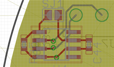
I'm designing a circular board with a BGA and lots of different IC's on it and I'm having various problems. I'll start with my first one, regarding Blind Via Ratio error in DRC:


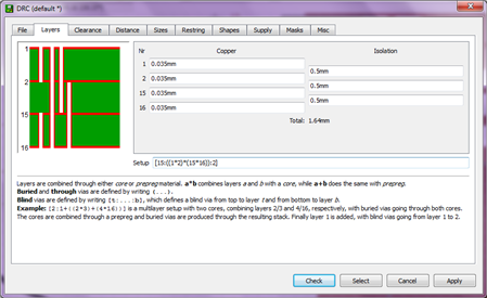
Layers setup in DRC:
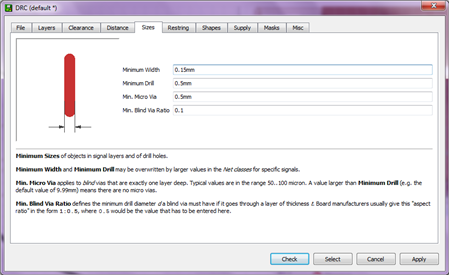
image

Sizes setup in DRC:

image


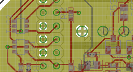
I end up with these warnings everywhere:

image


I have a number of other issues, but I thought I'd take them one at a time. Any help is very much appreciated!


Regards,

Peter Hygren

  • Sign in to reply
  • Cancel
Parents
  • Richard_H
    Richard_H over 15 years ago

    Hi Peter,


    the problem seems to be in the settings for Sizes in the Design Rules. You have 0.5mm for micro vias and for 'normal' vias. This does not allow EAGLE to dinstinguish between them and I suppose this is the reason for the errors. Usually the value for normal vias is higher than for micro vias. As far as I can see it from your Desing Rule settings, I think you don't use real micro vias. What happens if you decrease the micro vias value?


    Regards,

    Richard


    For further evaluation it would be good to send me your board file by email.

    • Cancel
    • Vote Up 0 Vote Down
    • Sign in to reply
    • Cancel
  • Former Member
    Former Member over 15 years ago in reply to Richard_H

    I changed my layer settings to only have one via type and the problem went away, on to a much more urgent problem:


    I have a supply layer (GND) that doesn't behave like it should regarding clearing room for vias and THT pins:

    (brown is GND plane obviously)
    image

    My layers:

    image

    And the GND layer:

    image

    The fill layer does however treat ground pins/vias correctly:

    image

    I need help urgently to solve this matter, any help is deeply appreciated. I'll send brd file on request via mail.

    • Cancel
    • Vote Up 0 Vote Down
    • Sign in to reply
    • Cancel
  • Former Member
    Former Member over 15 years ago in reply to Former Member

    BUMP

    Hasn't anyone else run into this problem?

    • Cancel
    • Vote Up 0 Vote Down
    • Sign in to reply
    • Cancel
Reply
  • Former Member
    Former Member over 15 years ago in reply to Former Member

    BUMP

    Hasn't anyone else run into this problem?

    • Cancel
    • Vote Up 0 Vote Down
    • Sign in to reply
    • Cancel
Children
No Data
element14 Community

element14 is the first online community specifically for engineers. Connect with your peers and get expert answers to your questions.

  • Members
  • Learn
  • Technologies
  • Challenges & Projects
  • Products
  • Store
  • About Us
  • Feedback & Support
  • FAQs
  • Terms of Use
  • Privacy Policy
  • Legal and Copyright Notices
  • Sitemap
  • Cookies

An Avnet Company © 2025 Premier Farnell Limited. All Rights Reserved.

Premier Farnell Ltd, registered in England and Wales (no 00876412), registered office: Farnell House, Forge Lane, Leeds LS12 2NE.

ICP 备案号 10220084.

Follow element14

  • X
  • Facebook
  • linkedin
  • YouTube