element14 Community
element14 Community
    Register Log In
  • Site
  • Search
  • Log In Register
  • Community Hub
    Community Hub
    • What's New on element14
    • Feedback and Support
    • Benefits of Membership
    • Personal Blogs
    • Members Area
    • Achievement Levels
  • Learn
    Learn
    • Ask an Expert
    • eBooks
    • element14 presents
    • Learning Center
    • Tech Spotlight
    • STEM Academy
    • Webinars, Training and Events
    • Learning Groups
  • Technologies
    Technologies
    • 3D Printing
    • FPGA
    • Industrial Automation
    • Internet of Things
    • Power & Energy
    • Sensors
    • Technology Groups
  • Challenges & Projects
    Challenges & Projects
    • Design Challenges
    • element14 presents Projects
    • Project14
    • Arduino Projects
    • Raspberry Pi Projects
    • Project Groups
  • Products
    Products
    • Arduino
    • Avnet & Tria Boards Community
    • Dev Tools
    • Manufacturers
    • Multicomp Pro
    • Product Groups
    • Raspberry Pi
    • RoadTests & Reviews
  • About Us
  • Store
    Store
    • Visit Your Store
    • Choose another store...
      • Europe
      •  Austria (German)
      •  Belgium (Dutch, French)
      •  Bulgaria (Bulgarian)
      •  Czech Republic (Czech)
      •  Denmark (Danish)
      •  Estonia (Estonian)
      •  Finland (Finnish)
      •  France (French)
      •  Germany (German)
      •  Hungary (Hungarian)
      •  Ireland
      •  Israel
      •  Italy (Italian)
      •  Latvia (Latvian)
      •  
      •  Lithuania (Lithuanian)
      •  Netherlands (Dutch)
      •  Norway (Norwegian)
      •  Poland (Polish)
      •  Portugal (Portuguese)
      •  Romania (Romanian)
      •  Russia (Russian)
      •  Slovakia (Slovak)
      •  Slovenia (Slovenian)
      •  Spain (Spanish)
      •  Sweden (Swedish)
      •  Switzerland(German, French)
      •  Turkey (Turkish)
      •  United Kingdom
      • Asia Pacific
      •  Australia
      •  China
      •  Hong Kong
      •  India
      •  Korea (Korean)
      •  Malaysia
      •  New Zealand
      •  Philippines
      •  Singapore
      •  Taiwan
      •  Thailand (Thai)
      • Americas
      •  Brazil (Portuguese)
      •  Canada
      •  Mexico (Spanish)
      •  United States
      Can't find the country/region you're looking for? Visit our export site or find a local distributor.
  • Translate
  • Profile
  • Settings
Autodesk EAGLE
  • Products
  • More
Autodesk EAGLE
Forum bench power supply
  • Blog
  • Forum
  • Documents
  • Events
  • Polls
  • Files
  • Members
  • Mentions
  • Sub-Groups
  • Tags
  • More
  • Cancel
  • New
Join Autodesk EAGLE to participate - click to join for free!
Actions
  • Share
  • More
  • Cancel
Forum Thread Details
  • State Verified Answer
  • Replies 42 replies
  • Answers 20 answers
  • Subscribers 179 subscribers
  • Views 6991 views
  • Users 0 members are here
Related

bench power supply

aster94
aster94 over 8 years ago

hello,


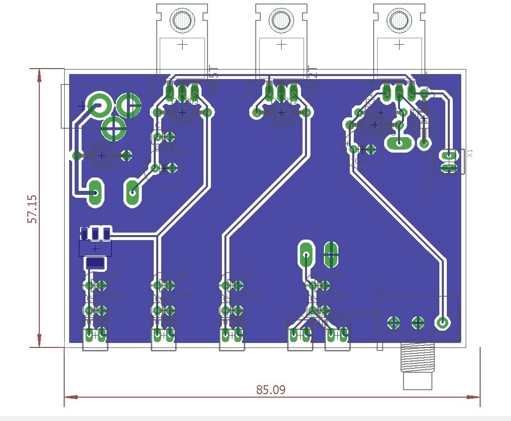
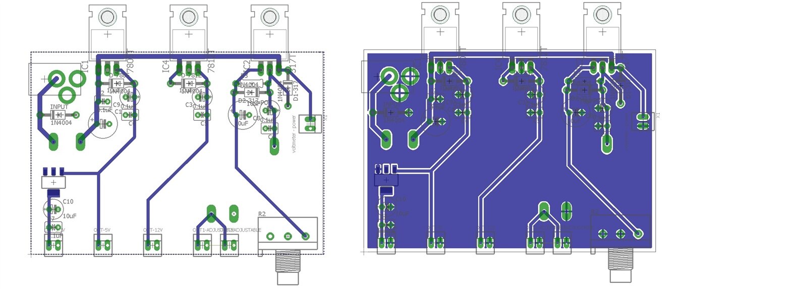
I started drawing in eagle this afternoon to make my first home made pbc board for a bench power supply that with an input of 12V/5A will have two output of 12V, 5V, 3.3V and an adjustable voltage (lm317)

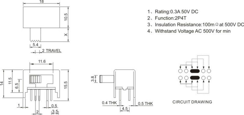
the switches are these with ground in the middle

565935243_150.jpg

I hope that the schematic is clear (it is also in the attachments), maybe you could give me some hint or advice about something that i m doing wrong

about the .brd i didn't route it since maybe you will say me to modify my schematic


thanks in advance


Immagine.png

Attachments:
bps.rar
  • Sign in to reply
  • Cancel

Top Replies

  • COMPACT
    COMPACT over 8 years ago in reply to mcb1 +3 suggested
    Here is an example of what I mean. 8V in from a regulated power supply being output as 5VDC using an LM7805 Linear Regulator. (The current limit has been set to 50mA on the bench power supply as not to…
  • mcb1
    mcb1 over 8 years ago in reply to aster94 +2 suggested
    the rated current it is 0.5 at 50v so I could reach 2A at 12v It doesn't work that way. The current specifies how much the switch will pass without damaging the contacts. The voltage specifies how high…
  • aster94
    aster94 over 8 years ago in reply to mcb1 +2
    As it is clear I am an hobbyist, thanks for the hint about the current In your schematics the middle pin of the potentiometer is not connected, is it correct? Is this schematic also good? http://www.electronics…
Parents
  • aster94
    0 aster94 over 8 years ago

    follow up:

    i hope that with this post i won't be seen as arrogant since I didn't use the schematic from @geralds

    His draw is obviously far away better than mine, but my main desire was to do this bench power supply on my own


    I completed the board in only one side, i used extra isolation for the ground plane than needed since i m not sure about our homemade etching quality


    image


    Now i will just have to wait for the 7812 then i will finish it image

    P.S: I know that the ground plane is not perfect near the lm317's outputs i will put a jumper

    • Cancel
    • Vote Up 0 Vote Down
    • Sign in to reply
    • Verify Answer
    • Cancel
  • COMPACT
    0 COMPACT over 8 years ago in reply to aster94

    Vincenzo,


    You seem to be focused on ancillary considerations and not the primary considerations as I've tried to lead you.


    Don't concern yourself about using power plane fills but get the essentials in order first.


    Here are some observations.


    1. PCB traces are too thin; they need to be thick enough to handle the envisaged current and be thick enough firstly to avoid acting as an unwanted fuse and handling the envisaged load.


    2.Your low impedance, small capacitance (100n) capacitors for the voltage regulator outputs are far too far away from the voltage regulators; ideally they should be adjacent.


    Have a look at Steve Ciarcia's Circuit Cellar How to build your own Z80 computer book which is available online which has a great section on power supplies for beginners.


    https://books.google.com.au/books?id=mVQnFgWzX0AC&printsec=frontcover&source=gbs_ge_summary_r&cad=0#v=onepage&q&f=false

    • Cancel
    • Vote Up 0 Vote Down
    • Sign in to reply
    • Verify Answer
    • Reject Answer
    • Cancel
  • aster94
    0 aster94 over 8 years ago in reply to COMPACT

    "You seem to be focused on ancillary considerations and not the primary considerations as I've tried to lead you."

    you are right i was so focused to connect all the components in the board that i forgot to give an appropriate width to the tracks, I used this calculator: The CircuitCalculator.com Blog » PCB Trace Width Calculator  and i used 50mil for the main power lines before the ICs and 32mil after the ICs since techinically the max amp after them should be <1.5 amp


    about the capacitors i really misunderstood a previous post, i thought that they had to stay as near as possible to the outputs....

    now i think it is correct


    image

    • Cancel
    • Vote Up 0 Vote Down
    • Sign in to reply
    • Verify Answer
    • Cancel
Reply
  • aster94
    0 aster94 over 8 years ago in reply to COMPACT

    "You seem to be focused on ancillary considerations and not the primary considerations as I've tried to lead you."

    you are right i was so focused to connect all the components in the board that i forgot to give an appropriate width to the tracks, I used this calculator: The CircuitCalculator.com Blog » PCB Trace Width Calculator  and i used 50mil for the main power lines before the ICs and 32mil after the ICs since techinically the max amp after them should be <1.5 amp


    about the capacitors i really misunderstood a previous post, i thought that they had to stay as near as possible to the outputs....

    now i think it is correct


    image

    • Cancel
    • Vote Up 0 Vote Down
    • Sign in to reply
    • Verify Answer
    • Cancel
Children
  • geralds
    0 geralds over 8 years ago in reply to aster94

    Hi,


    fine, congratulations!


    A little bit:

    1) place the output connectors and poti also the V-regulators a bit to inside of the board, then you have a closed GND plane with this polygon.

    Then you don't need wire jumpers.


    2) turn the input plug backwards to the IC side then you can make a small enclosure around the PCB that have on the front- and backside the mounting parts but not on the l/r sides.


    The 100n bypass capacitors have mounting so close to the ICs as you can. They are ceramic capacitors, withstanding > 50V.


    Best Regards,

    Gerald

    ---

    • Cancel
    • Vote Up 0 Vote Down
    • Sign in to reply
    • Verify Answer
    • Reject Answer
    • Cancel
element14 Community

element14 is the first online community specifically for engineers. Connect with your peers and get expert answers to your questions.

  • Members
  • Learn
  • Technologies
  • Challenges & Projects
  • Products
  • Store
  • About Us
  • Feedback & Support
  • FAQs
  • Terms of Use
  • Privacy Policy
  • Legal and Copyright Notices
  • Sitemap
  • Cookies

An Avnet Company © 2025 Premier Farnell Limited. All Rights Reserved.

Premier Farnell Ltd, registered in England and Wales (no 00876412), registered office: Farnell House, Forge Lane, Leeds LS12 2NE.

ICP 备案号 10220084.

Follow element14

  • X
  • Facebook
  • linkedin
  • YouTube