element14 Community
element14 Community
    Register Log In
  • Site
  • Search
  • Log In Register
  • About Us
  • Community Hub
    Community Hub
    • What's New on element14
    • Feedback and Support
    • Benefits of Membership
    • Personal Blogs
    • Members Area
    • Achievement Levels
  • Learn
    Learn
    • Ask an Expert
    • eBooks
    • element14 presents
    • Learning Center
    • Tech Spotlight
    • STEM Academy
    • Webinars, Training and Events
    • Learning Groups
  • Technologies
    Technologies
    • 3D Printing
    • FPGA
    • Industrial Automation
    • Internet of Things
    • Power & Energy
    • Sensors
    • Technology Groups
  • Challenges & Projects
    Challenges & Projects
    • Design Challenges
    • element14 presents Projects
    • Project14
    • Arduino Projects
    • Raspberry Pi Projects
    • Project Groups
  • Products
    Products
    • Arduino
    • Avnet Boards Community
    • Dev Tools
    • Manufacturers
    • Multicomp Pro
    • Product Groups
    • Raspberry Pi
    • RoadTests & Reviews
  • Store
    Store
    • Visit Your Store
    • Choose another store...
      • Europe
      •  Austria (German)
      •  Belgium (Dutch, French)
      •  Bulgaria (Bulgarian)
      •  Czech Republic (Czech)
      •  Denmark (Danish)
      •  Estonia (Estonian)
      •  Finland (Finnish)
      •  France (French)
      •  Germany (German)
      •  Hungary (Hungarian)
      •  Ireland
      •  Israel
      •  Italy (Italian)
      •  Latvia (Latvian)
      •  
      •  Lithuania (Lithuanian)
      •  Netherlands (Dutch)
      •  Norway (Norwegian)
      •  Poland (Polish)
      •  Portugal (Portuguese)
      •  Romania (Romanian)
      •  Russia (Russian)
      •  Slovakia (Slovak)
      •  Slovenia (Slovenian)
      •  Spain (Spanish)
      •  Sweden (Swedish)
      •  Switzerland(German, French)
      •  Turkey (Turkish)
      •  United Kingdom
      • Asia Pacific
      •  Australia
      •  China
      •  Hong Kong
      •  India
      •  Korea (Korean)
      •  Malaysia
      •  New Zealand
      •  Philippines
      •  Singapore
      •  Taiwan
      •  Thailand (Thai)
      • Americas
      •  Brazil (Portuguese)
      •  Canada
      •  Mexico (Spanish)
      •  United States
      Can't find the country/region you're looking for? Visit our export site or find a local distributor.
  • Translate
  • Profile
  • Settings
Altium CircuitStudio
  • Products
  • Manufacturers
  • Altium CircuitStudio
  • More
  • Cancel
Altium CircuitStudio
Altium CircuitStudio Forum Selective thermal relief for thru holes, smt pads, vias in CircuitStudio?
  • Blog
  • Forum
  • Documents
  • Events
  • Polls
  • Members
  • Mentions
  • Sub-Groups
  • Tags
  • More
  • Cancel
  • New
Join Altium CircuitStudio to participate - click to join for free!
Actions
  • Share
  • More
  • Cancel
Forum Thread Details
  • State Verified Answer
  • Locked Locked
  • Replies 10 replies
  • Answers 4 answers
  • Subscribers 93 subscribers
  • Views 3992 views
  • Users 0 members are here
Related
This discussion has been locked.
You can no longer post new replies to this discussion. If you have a question you can start a new discussion

Selective thermal relief for thru holes, smt pads, vias in CircuitStudio?

nszmnsky
nszmnsky over 8 years ago

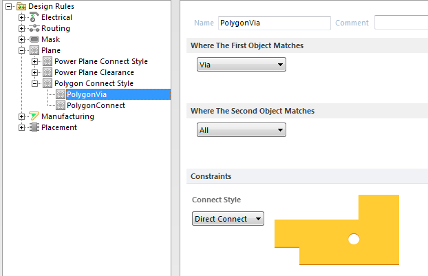
I often need to change the connection of a polygon depending on what connecting to - for instance, often want direct for vias but X on smt pads. Can this be done in CS? I don't see a way to configure rule for anything other than net, no option for setting what its connecting to.


Thanks

Neil

  • Cancel

Top Replies

  • michaelwylie
    michaelwylie over 8 years ago +1 suggested
    Check the design rules under Plane > Polygon Connect Style > Polygon Connect.
  • nszmnsky
    nszmnsky over 8 years ago in reply to michaelwylie +1 suggested
    I do not see an option to select different connect styles for different features. Only settings are for net and/or layer combinations. I want to not have thermal relief on vias but have them on thru holes…
  • michaelwylie
    0 michaelwylie over 8 years ago

    Check the design rules under Plane > Polygon Connect Style > Polygon Connect.

    • Cancel
    • Vote Up +1 Vote Down
    • Cancel
  • nszmnsky
    0 nszmnsky over 8 years ago in reply to michaelwylie

    I do not see an option to select different connect styles for different features. Only settings are for net and/or layer combinations. I want to not have thermal relief on vias but have them on thru holes for instance.

    image

    • Cancel
    • Vote Up +1 Vote Down
    • Cancel
  • michaelwylie
    0 michaelwylie over 8 years ago in reply to nszmnsky

    You might have to make an advanced rule. I'm not sure the query you would make though. Check out advanced Rules using the Rule Wizard.

    • Cancel
    • Vote Up 0 Vote Down
    • Cancel
  • harvie256
    0 harvie256 over 8 years ago

    The answer to this question using the built in CS tools is no.  Altium have removed some of the query stuff necessary from AD.  They made a mess of this in my opinion.


    However, given this is tool I bought and use, I needed to find a way.  So I manually edit rules outside of CS and re-import them, as the backend is still the same as AD and still works the same way.  See my question over at the eevblog forum for how I do it:

    http://www.eevblog.com/forum/altium/polygon-pour-connection-for-vias/


    As an example, below is the contents of the exported and modified .RUL file for no relief on vias, but relief on everything else:


    SELECTION=FALSE|LAYER=TOP|LOCKED=FALSE|POLYGONOUTLINE=FALSE|USERROUTED=TRUE|UNIONINDEX=0|RULEKIND=PolygonConnect|NETSCOPE=AnyNet|LAYERKIND=SameLayer|SCOPE1EXPRESSION=IsVia|SCOPE2EXPRESSION=All|NAME=PolygonConnect_Via|ENABLED=TRUE|PRIORITY=1|COMMENT= |UNIQUEID=YEEDPGAH|DEFINEDBYLOGICALDOCUMENT=FALSE|CONNECTSTYLE=Direct|RELIEFCONDUCTORWIDTH=10mil|RELIEFENTRIES=4|POLYGONRELIEFANGLE=90 Angle|AIRGAPWIDTH=10mil

    SELECTION=FALSE|LAYER=TOP|LOCKED=FALSE|POLYGONOUTLINE=FALSE|USERROUTED=TRUE|UNIONINDEX=0|RULEKIND=PolygonConnect|NETSCOPE=AnyNet|LAYERKIND=SameLayer|SCOPE1EXPRESSION=All|SCOPE2EXPRESSION=All|NAME=PolygonConnect_all|ENABLED=TRUE|PRIORITY=2|COMMENT= |UNIQUEID=IPIHNEGD|DEFINEDBYLOGICALDOCUMENT=FALSE|CONNECTSTYLE=Relief|RELIEFCONDUCTORWIDTH=10mil|RELIEFENTRIES=4|POLYGONRELIEFANGLE=45 Angle|AIRGAPWIDTH=10mil

    • Cancel
    • Vote Up 0 Vote Down
    • Cancel
  • nszmnsky
    0 nszmnsky over 8 years ago in reply to harvie256

    Thanks harvie256! IF I had a list of design rule options AND IF I wanted to manually create the rules I could accomplish what I need. I still have trouble wrapping my head around the use of rules to control PCB layout. I'm coming from NI Ultiboard where things such as reliefs, min width and spacing are Properties of the item, and each instance of the item can be individually manipulated. Want only one via direct connected? Just click on it and set the property. Want to set the relief style, spoke, and air gap of a polygon? Just click on it and set all those properties in one place. Problem is I haven't upgrade Ultiboard for a few years so have been evaluating other PCB packages to see if I should switch. I do like CS's ability to import from other PCB packages like Eagle as well as from Designer (by exporting as previous version). Of the PCB packages I've looked at, CS has the most plus's  - just not sure enough of them.

    • Cancel
    • Vote Up 0 Vote Down
    • Cancel
  • batuu
    0 batuu over 8 years ago in reply to harvie256

    As harvie256 said, they removed some helpful things, but the underlaying engine is still there. Same fate for concepts like object classes like net classes or component classes. I hope, altium reconsider this and bring this tools back in release 2.0.

    • Cancel
    • Vote Up 0 Vote Down
    • Cancel
  • Former Member
    0 Former Member over 8 years ago

    You can make Circuit Studio connect a via to a polygon pour directly and have thermal reliefs for your other pads. It takes a bit of effort though. I made a tutorial here: http://www.eevblog.com/forum/circuit-studio/how-to-selective-thermal-relief-for-vias-and-pads/

    • Cancel
    • Vote Up 0 Vote Down
    • Cancel
  • adamwebber
    0 adamwebber over 8 years ago in reply to Former Member

    Thank You Thank You Thank You for explaining design rules to me.  Transitioning from Altium to CircuitStudio has been a little frustrating but now that I understand CircuitStudio is Altium and I just need to use the workarounds, everything is still possible.  I love the interface of CS better than Altium but I don't like all of the items that have been removed.  This discussion has been a huge help.


    I used to use the command IsVia in Altium while declaring polygon connect rules and for CS I have two methods of relief-connects and direct-connects using polygon pours.

    1-Declare everything as a direct-connect unless it is a component.  Priority is key.

    2-Export the Rules, edit them and Import them back in.  Unless you know how to use Altium, this can be difficult.


    If someone else is looking for this, I hope that they find it.  I had difficulty searching through the forums.

    • Cancel
    • Vote Up 0 Vote Down
    • Cancel
  • lamabrew
    0 lamabrew over 7 years ago in reply to Former Member

    For anyone else that comes across this, in 1.4 you can now select vias for the match. I did it like this, YMMV.

    image

    • Cancel
    • Vote Up 0 Vote Down
    • Cancel
  • chuckjls
    0 chuckjls over 5 years ago in reply to nszmnsky

    Thanks for the help. This is by far the easiest way to get rid of the thermals.

    • Cancel
    • Vote Up 0 Vote Down
    • Cancel
element14 Community

element14 is the first online community specifically for engineers. Connect with your peers and get expert answers to your questions.

  • Members
  • Learn
  • Technologies
  • Challenges & Projects
  • Products
  • Store
  • About Us
  • Feedback & Support
  • FAQs
  • Terms of Use
  • Privacy Policy
  • Legal and Copyright Notices
  • Sitemap
  • Cookies

An Avnet Company © 2025 Premier Farnell Limited. All Rights Reserved.

Premier Farnell Ltd, registered in England and Wales (no 00876412), registered office: Farnell House, Forge Lane, Leeds LS12 2NE.

ICP 备案号 10220084.

Follow element14

  • X
  • Facebook
  • linkedin
  • YouTube