element14 Community
element14 Community
    Register Log In
  • Site
  • Search
  • Log In Register
  • Community Hub
    Community Hub
    • What's New on element14
    • Feedback and Support
    • Benefits of Membership
    • Personal Blogs
    • Members Area
    • Achievement Levels
  • Learn
    Learn
    • Ask an Expert
    • eBooks
    • element14 presents
    • Learning Center
    • Tech Spotlight
    • STEM Academy
    • Webinars, Training and Events
    • Learning Groups
  • Technologies
    Technologies
    • 3D Printing
    • FPGA
    • Industrial Automation
    • Internet of Things
    • Power & Energy
    • Sensors
    • Technology Groups
  • Challenges & Projects
    Challenges & Projects
    • Design Challenges
    • element14 presents Projects
    • Project14
    • Arduino Projects
    • Raspberry Pi Projects
    • Project Groups
  • Products
    Products
    • Arduino
    • Avnet Boards Community
    • Dev Tools
    • Manufacturers
    • Multicomp Pro
    • Product Groups
    • Raspberry Pi
    • RoadTests & Reviews
  • Store
    Store
    • Visit Your Store
    • Choose another store...
      • Europe
      •  Austria (German)
      •  Belgium (Dutch, French)
      •  Bulgaria (Bulgarian)
      •  Czech Republic (Czech)
      •  Denmark (Danish)
      •  Estonia (Estonian)
      •  Finland (Finnish)
      •  France (French)
      •  Germany (German)
      •  Hungary (Hungarian)
      •  Ireland
      •  Israel
      •  Italy (Italian)
      •  Latvia (Latvian)
      •  
      •  Lithuania (Lithuanian)
      •  Netherlands (Dutch)
      •  Norway (Norwegian)
      •  Poland (Polish)
      •  Portugal (Portuguese)
      •  Romania (Romanian)
      •  Russia (Russian)
      •  Slovakia (Slovak)
      •  Slovenia (Slovenian)
      •  Spain (Spanish)
      •  Sweden (Swedish)
      •  Switzerland(German, French)
      •  Turkey (Turkish)
      •  United Kingdom
      • Asia Pacific
      •  Australia
      •  China
      •  Hong Kong
      •  India
      •  Korea (Korean)
      •  Malaysia
      •  New Zealand
      •  Philippines
      •  Singapore
      •  Taiwan
      •  Thailand (Thai)
      • Americas
      •  Brazil (Portuguese)
      •  Canada
      •  Mexico (Spanish)
      •  United States
      Can't find the country/region you're looking for? Visit our export site or find a local distributor.
  • Translate
  • Profile
  • Settings
Altium CircuitStudio
  • Products
  • Manufacturers
  • Altium CircuitStudio
  • More
  • Cancel
Altium CircuitStudio
Altium CircuitStudio Forum Board Outlines - How to Double Check
  • Blog
  • Forum
  • Documents
  • Events
  • Polls
  • Members
  • Mentions
  • Sub-Groups
  • Tags
  • More
  • Cancel
  • New
Join Altium CircuitStudio to participate - click to join for free!
Actions
  • Share
  • More
  • Cancel
Forum Thread Details
  • State Not Answered
  • Locked Locked
  • Replies 7 replies
  • Subscribers 88 subscribers
  • Views 602 views
  • Users 0 members are here
  • frontpage
Related
This discussion has been locked.
You can no longer post new replies to this discussion. If you have a question you can start a new discussion

Board Outlines - How to Double Check

baudot
baudot over 7 years ago

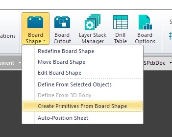
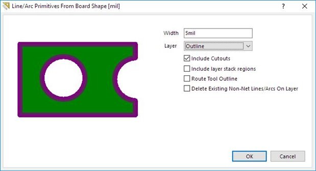
What tools outside CircuitStudio can I use to check my board outlines for correctness?


My issue: After I output my design to gerbers, zip those up, and upload to Osh Park, I get the message back that my board outline is a mere 0.04 x 0.07 inches. The board outline I set up during editing is 600x600 mils, so that shouldn't be correct. Osh Park support reports that the outline file doesn't contain the board outline at all: It only has the pad for a single resistor in it. Looking over the outline file in this online tool backs up Osh Park's assertion: I see the pad for one of the board resistors, not a board outline.


What could cause this sort of error when outputting to gerbers?

  • Cancel

Top Replies

  • bugrobotics
    bugrobotics over 7 years ago in reply to baudot +2
    HI Sam, You can use "Board Shape" ->"Create Primitives from Board Shape" then select "Outline" layer to create your board outline quickly without having to trace anything. This comes in handy with non…
  • bugrobotics
    bugrobotics over 7 years ago in reply to baudot +2
    Hi Sam, Yea, it's the intended workflow. The options allow the user to include cutouts as well as delete random lines on the outline layer. These are pretty important if you have some funky cutouts and…
  • baudot
    baudot over 7 years ago in reply to genebren +1
    In fact that's the same one I already linked that appeared to confirm the vendor's claim of the outline being messed up. Any other ideas what could be causing the failure or other recommended tools to…
  • genebren
    0 genebren over 7 years ago

    Sam,


    There are several free gerber file viewers that can be used to confirm your files.  There is a fair degree of looseness out there on how files are interpreted and I to have had several instances where a vendor claims my files are wrong, when in fact they are fine.


    Here is a free online viewer that might be helpful in tracking down the problem.

    Online Gerber Viewer


    Good luck,

    Gene

    • Cancel
    • Vote Up 0 Vote Down
    • Cancel
  • baudot
    0 baudot over 7 years ago in reply to genebren

    In fact that's the same one I already linked that appeared to confirm the vendor's claim of the outline being messed up.


    Any other ideas what could be causing the failure or other recommended tools to investigate with?

    • Cancel
    • Vote Up +1 Vote Down
    • Cancel
  • genebren
    0 genebren over 7 years ago in reply to baudot

    Sam,


    Yeah, I kind of noticed that you had used the same viewer that I mentioned after I hit reply.  Oh well.  I am not familiar enough with CircuitStudio to help you get past this, but do not worry, there are a lot of people here who seem to be using this package, so hopefully someone will see your post and help you out.


    Good luck,

    Gene

    • Cancel
    • Vote Up 0 Vote Down
    • Cancel
  • baudot
    0 baudot over 7 years ago in reply to genebren

    Thanks for the reply, all the same. If nothing else, we made the board active for a bit, eh?

    I did later get the solution. It was easy yet counterintuitive:


    The "board shape" feature of CircuitStudio doesn't actually define the board shape! You still have to select the "Outline" layer of the board and trace over the shape you intend to draw. That's all it was.

    • Cancel
    • Vote Up +1 Vote Down
    • Cancel
  • bugrobotics
    0 bugrobotics over 7 years ago in reply to baudot

    HI Sam,

    You can use "Board Shape" ->"Create Primitives from Board Shape" then select "Outline" layer to create your board outline quickly without having to trace anything.  This comes in handy with non-rectangular boards.


    image

    image

    • Cancel
    • Vote Up +2 Vote Down
    • Cancel
  • baudot
    0 baudot over 7 years ago in reply to bugrobotics

    Thank you. This is very helpful.


    Do you know if this is the intended workflow? I found it very counter-intuitive that the board shape wasn't automatically used as the outline. It seems deceptive to have the user define a board shape and then add extra steps to actually use the shape once it's been set up.

    • Cancel
    • Vote Up +1 Vote Down
    • Cancel
  • bugrobotics
    0 bugrobotics over 7 years ago in reply to baudot

    Hi Sam,

    Yea, it's the intended workflow.  The options allow the user to include cutouts as well as delete random lines on the outline layer.  These are pretty important if you have some funky cutouts and/or made a mistake at 3AM while routing your board and accidentally placed a few traces on the outline layer (image).

    • Cancel
    • Vote Up +2 Vote Down
    • Cancel
element14 Community

element14 is the first online community specifically for engineers. Connect with your peers and get expert answers to your questions.

  • Members
  • Learn
  • Technologies
  • Challenges & Projects
  • Products
  • Store
  • About Us
  • Feedback & Support
  • FAQs
  • Terms of Use
  • Privacy Policy
  • Legal and Copyright Notices
  • Sitemap
  • Cookies

An Avnet Company © 2025 Premier Farnell Limited. All Rights Reserved.

Premier Farnell Ltd, registered in England and Wales (no 00876412), registered office: Farnell House, Forge Lane, Leeds LS12 2NE.

ICP 备案号 10220084.

Follow element14

  • X
  • Facebook
  • linkedin
  • YouTube