element14 Community
element14 Community
    Register Log In
  • Site
  • Search
  • Log In Register
  • Community Hub
    Community Hub
    • What's New on element14
    • Feedback and Support
    • Benefits of Membership
    • Personal Blogs
    • Members Area
    • Achievement Levels
  • Learn
    Learn
    • Ask an Expert
    • eBooks
    • element14 presents
    • Learning Center
    • Tech Spotlight
    • STEM Academy
    • Webinars, Training and Events
    • Learning Groups
  • Technologies
    Technologies
    • 3D Printing
    • FPGA
    • Industrial Automation
    • Internet of Things
    • Power & Energy
    • Sensors
    • Technology Groups
  • Challenges & Projects
    Challenges & Projects
    • Design Challenges
    • element14 presents Projects
    • Project14
    • Arduino Projects
    • Raspberry Pi Projects
    • Project Groups
  • Products
    Products
    • Arduino
    • Avnet Boards Community
    • Dev Tools
    • Manufacturers
    • Multicomp Pro
    • Product Groups
    • Raspberry Pi
    • RoadTests & Reviews
  • Store
    Store
    • Visit Your Store
    • Choose another store...
      • Europe
      •  Austria (German)
      •  Belgium (Dutch, French)
      •  Bulgaria (Bulgarian)
      •  Czech Republic (Czech)
      •  Denmark (Danish)
      •  Estonia (Estonian)
      •  Finland (Finnish)
      •  France (French)
      •  Germany (German)
      •  Hungary (Hungarian)
      •  Ireland
      •  Israel
      •  Italy (Italian)
      •  Latvia (Latvian)
      •  
      •  Lithuania (Lithuanian)
      •  Netherlands (Dutch)
      •  Norway (Norwegian)
      •  Poland (Polish)
      •  Portugal (Portuguese)
      •  Romania (Romanian)
      •  Russia (Russian)
      •  Slovakia (Slovak)
      •  Slovenia (Slovenian)
      •  Spain (Spanish)
      •  Sweden (Swedish)
      •  Switzerland(German, French)
      •  Turkey (Turkish)
      •  United Kingdom
      • Asia Pacific
      •  Australia
      •  China
      •  Hong Kong
      •  India
      •  Korea (Korean)
      •  Malaysia
      •  New Zealand
      •  Philippines
      •  Singapore
      •  Taiwan
      •  Thailand (Thai)
      • Americas
      •  Brazil (Portuguese)
      •  Canada
      •  Mexico (Spanish)
      •  United States
      Can't find the country/region you're looking for? Visit our export site or find a local distributor.
  • Translate
  • Profile
  • Settings
Altium CircuitStudio
  • Products
  • Manufacturers
  • Altium CircuitStudio
  • More
  • Cancel
Altium CircuitStudio
Altium CircuitStudio Forum Route to a pad
  • Blog
  • Forum
  • Documents
  • Events
  • Polls
  • Members
  • Mentions
  • Sub-Groups
  • Tags
  • More
  • Cancel
  • New
Join Altium CircuitStudio to participate - click to join for free!
Actions
  • Share
  • More
  • Cancel
Forum Thread Details
  • State Verified Answer
  • Locked Locked
  • Replies 5 replies
  • Answers 2 answers
  • Subscribers 88 subscribers
  • Views 1869 views
  • Users 0 members are here
  • routing
Related
This discussion has been locked.
You can no longer post new replies to this discussion. If you have a question you can start a new discussion

Route to a pad

baudot
baudot over 7 years ago

I'm trying to make an ultra-simple break-out board: Every pin on a surface-mount chip goes to a pad on a PCB, so I can solder male headers into the pads for easy prototyping on a solderless breadboard.


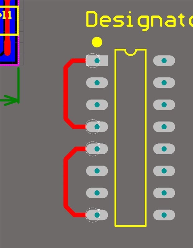
The problem is, when I try to route from the chip's pins to the pads, the route dodges the pad! (See attached image.)

The mouse acquires a symbol, crossed wires, when I try to make the connection. (For reasons unknown, my screen-grab tool doesn't grab it.)


My suspicion is that since the pad was added in the PCB editor, and the schematic is literally just the chip, with no connections, the PCB editor thinks it should indeed be a floating pin, connected to nothing.


How do I get around this? How do I route from a chip to a pad that I've added in the PCB editor window?

Attachments:
image
  • Cancel
  • baudot
    0 baudot over 7 years ago

    Workaround in this case: Remove the pads from the PCB, add headers as a component to the schematic, and wire them together.


    Still, what's the point of being able to add pads on the fly in the PCB editor if you can't connect to them? Surely you can, and I'm missing something?

    • Cancel
    • Vote Up 0 Vote Down
    • Cancel
  • voltsandjolts
    0 voltsandjolts over 7 years ago in reply to baudot

    As you don't have a full schematic that means you probably don't have any nets defined either. You can't connect to the pad because it is not assigned to the net of the track you are editing. You can double click each pad and assign a net for it. You can get the net name from the tracks you create or create all nets in Tools> Netlist > Edit. Probably easier just to create your pad layout as a component and do a proper schematic. 10 mins.

    • Cancel
    • Vote Up 0 Vote Down
    • Cancel
  • mars01
    0 mars01 over 7 years ago

    I recommend to do what the previous answers said but if you really, really want to do what you proposed to do then go to: File -> System Preferences -> PCB Editor -> Routing Conflict Resolutions -> Current Mode and in the drop-down menu select Ignore obstacles. This will allow you to cross with the track over a pad not in the same net. You'll see the connections marked with a white circle and shortcircuit symbol but it will work if the only thing you want is to do a toner transfer PCB image


    image

    • Cancel
    • Vote Up 0 Vote Down
    • Cancel
  • e14softwareuk
    0 e14softwareuk over 7 years ago in reply to mars01

    To add to this suggestion of using Ignore Obstacles, once you have completed your routing use Tools | Netlist > Configure Physical Nets. This brings up a dialog that lets you turn the copper into actual nets. Gets rid of the short circuit indicators.

    • Cancel
    • Vote Up 0 Vote Down
    • Cancel
  • baudot
    0 baudot over 7 years ago in reply to voltsandjolts

    Thanks. As a new user, it took me a bit to figure out one or two less obvious things about this. (Mostly that I had to add a 0-length unlabeled pin to the pad to make it a connection point.)


    This answer got me where I needed to be.

    • Cancel
    • Vote Up 0 Vote Down
    • Cancel
element14 Community

element14 is the first online community specifically for engineers. Connect with your peers and get expert answers to your questions.

  • Members
  • Learn
  • Technologies
  • Challenges & Projects
  • Products
  • Store
  • About Us
  • Feedback & Support
  • FAQs
  • Terms of Use
  • Privacy Policy
  • Legal and Copyright Notices
  • Sitemap
  • Cookies

An Avnet Company © 2025 Premier Farnell Limited. All Rights Reserved.

Premier Farnell Ltd, registered in England and Wales (no 00876412), registered office: Farnell House, Forge Lane, Leeds LS12 2NE.

ICP 备案号 10220084.

Follow element14

  • X
  • Facebook
  • linkedin
  • YouTube