element14 Community
element14 Community
    Register Log In
  • Site
  • Search
  • Log In Register
  • Community Hub
    Community Hub
    • What's New on element14
    • Feedback and Support
    • Benefits of Membership
    • Personal Blogs
    • Members Area
    • Achievement Levels
  • Learn
    Learn
    • Ask an Expert
    • eBooks
    • element14 presents
    • Learning Center
    • Tech Spotlight
    • STEM Academy
    • Webinars, Training and Events
    • Learning Groups
  • Technologies
    Technologies
    • 3D Printing
    • FPGA
    • Industrial Automation
    • Internet of Things
    • Power & Energy
    • Sensors
    • Technology Groups
  • Challenges & Projects
    Challenges & Projects
    • Design Challenges
    • element14 presents Projects
    • Project14
    • Arduino Projects
    • Raspberry Pi Projects
    • Project Groups
  • Products
    Products
    • Arduino
    • Avnet & Tria Boards Community
    • Dev Tools
    • Manufacturers
    • Multicomp Pro
    • Product Groups
    • Raspberry Pi
    • RoadTests & Reviews
  • About Us
  • Store
    Store
    • Visit Your Store
    • Choose another store...
      • Europe
      •  Austria (German)
      •  Belgium (Dutch, French)
      •  Bulgaria (Bulgarian)
      •  Czech Republic (Czech)
      •  Denmark (Danish)
      •  Estonia (Estonian)
      •  Finland (Finnish)
      •  France (French)
      •  Germany (German)
      •  Hungary (Hungarian)
      •  Ireland
      •  Israel
      •  Italy (Italian)
      •  Latvia (Latvian)
      •  
      •  Lithuania (Lithuanian)
      •  Netherlands (Dutch)
      •  Norway (Norwegian)
      •  Poland (Polish)
      •  Portugal (Portuguese)
      •  Romania (Romanian)
      •  Russia (Russian)
      •  Slovakia (Slovak)
      •  Slovenia (Slovenian)
      •  Spain (Spanish)
      •  Sweden (Swedish)
      •  Switzerland(German, French)
      •  Turkey (Turkish)
      •  United Kingdom
      • Asia Pacific
      •  Australia
      •  China
      •  Hong Kong
      •  India
      •  Korea (Korean)
      •  Malaysia
      •  New Zealand
      •  Philippines
      •  Singapore
      •  Taiwan
      •  Thailand (Thai)
      • Americas
      •  Brazil (Portuguese)
      •  Canada
      •  Mexico (Spanish)
      •  United States
      Can't find the country/region you're looking for? Visit our export site or find a local distributor.
  • Translate
  • Profile
  • Settings
Altium CircuitStudio
  • Products
  • Manufacturers
  • Altium CircuitStudio
  • More
  • Cancel
Altium CircuitStudio
Altium CircuitStudio Forum Problem with hatched pour violating clearance setting
  • Blog
  • Forum
  • Documents
  • Events
  • Polls
  • Members
  • Mentions
  • Sub-Groups
  • Tags
  • More
  • Cancel
  • New
Join Altium CircuitStudio to participate - click to join for free!
Actions
  • Share
  • More
  • Cancel
Forum Thread Details
  • State Not Answered
  • Locked Locked
  • Replies 14 replies
  • Subscribers 88 subscribers
  • Views 2732 views
  • Users 0 members are here
  • frontpage
Related
This discussion has been locked.
You can no longer post new replies to this discussion. If you have a question you can start a new discussion

Problem with hatched pour violating clearance setting

chuckbluz
chuckbluz over 7 years ago

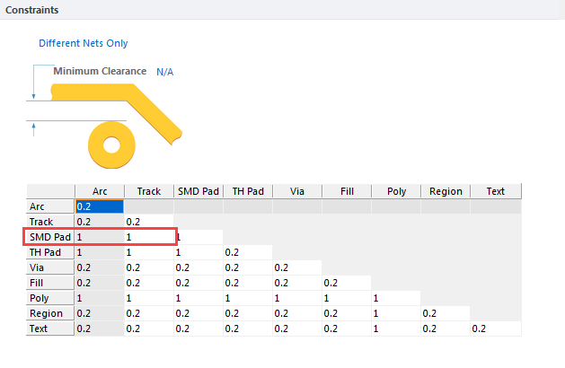
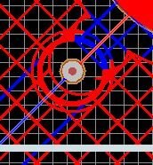
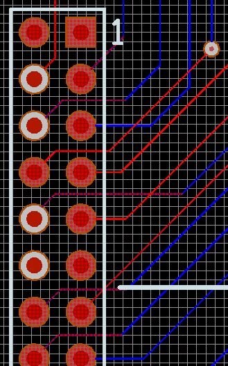
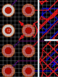
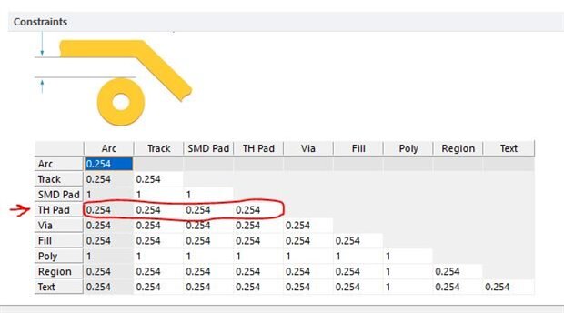
. I’m looking for help with hatched pours., I’m building a capacitive touch pcb, and need 1mm clearance around my touch pads., I’ve set the design rules accordingly. But this is what I get:


image

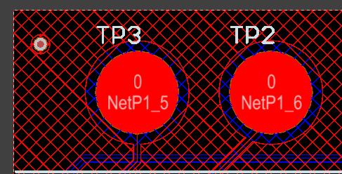
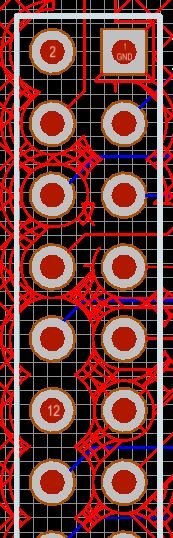
You can see that some of the hatching is actually inside the 1mm clearance. Of the 28 sensor pads I have laid out, only 1 is usable. This occurs with 45 degree and/or 90 degree hatching. I tried a solid pour, and that works fine.

Unfortunately, I must have a hatched pour.


I looked at the documentation PDFs, and the problem is there, and I also used an online gerber viewer, and verified the problem. I need to send files to our factory in China today, but I cannot send them with this problem.

  • Cancel
Parents
  • e14softwareuk
    0 e14softwareuk over 7 years ago

    Hi Charles. Unfortunately your linked image is not displaying. A couple of ideas - increase the clearance of the polygon to ensure >1mm; use a solid pour close to the buttons and hatch to fill the remainder; are the touch areas pads - if so check if using arcs or octagons to draw around pads.

    • Cancel
    • Vote Up 0 Vote Down
    • Cancel
  • chuckbluz
    0 chuckbluz over 7 years ago in reply to e14softwareuk

    I'm using arcs - I tried octagons, and have the same problem.

    • Cancel
    • Vote Up 0 Vote Down
    • Cancel
  • e14softwareuk
    0 e14softwareuk over 7 years ago in reply to chuckbluz

    In that case might be worth trying to increase the clearance by half the line width of the hatch.

    • Cancel
    • Vote Up 0 Vote Down
    • Cancel
Reply
  • e14softwareuk
    0 e14softwareuk over 7 years ago in reply to chuckbluz

    In that case might be worth trying to increase the clearance by half the line width of the hatch.

    • Cancel
    • Vote Up 0 Vote Down
    • Cancel
Children
  • chuckbluz
    0 chuckbluz over 7 years ago in reply to e14softwareuk

    The weird thing is if I use a solid pour, there are no problems. It's clearly an issue with hatched pours.

    • Cancel
    • Vote Up 0 Vote Down
    • Cancel
  • chuckbluz
    0 chuckbluz over 7 years ago in reply to chuckbluz

    I just tried your suggestion about increasing the clearance width----- it didn't work.

    • Cancel
    • Vote Up 0 Vote Down
    • Cancel
  • e14softwareuk
    0 e14softwareuk over 7 years ago in reply to chuckbluz

    Did the clearance change? If not then are you adjusting the correct clearance or do you have multiple rules and the wrong one is taking priority. From memory it is possible the hatched pours may draw the outline along the boundary and hence be 1/2 the line width closer than expected.

    • Cancel
    • Vote Up 0 Vote Down
    • Cancel
  • chuckbluz
    0 chuckbluz over 7 years ago in reply to e14softwareuk

    Yes, the clearance changed as expected. The problems I am seeing are greater than just 1/2 the line width. I just tried adding a keepout around one of the pads, repoured the hatch and the hatch went crazy - much of the hatch around that pad was missing or incomplete. Hopefully you can see the image. The problem is on every pad, some worse or better than others.(the image is of the hatch problem, not the attempt with the keepout!)

    .image

    • Cancel
    • Vote Up 0 Vote Down
    • Cancel
  • e14softwareuk
    0 e14softwareuk over 7 years ago in reply to chuckbluz

    Thanks for sharing the image. If you would like me to take a look at the design tomorrow please feel free to zip up the PCB and send through to software@element14.com.

    • Cancel
    • Vote Up 0 Vote Down
    • Cancel
  • chuckbluz
    0 chuckbluz over 7 years ago in reply to e14softwareuk

    That would be great thanks - it could be an operator error...:-) I'll send it to you shortly

    • Cancel
    • Vote Up 0 Vote Down
    • Cancel
  • e14softwareuk
    0 e14softwareuk over 7 years ago in reply to chuckbluz

    Hi Charles. Many thanks for sending through the design - I have investigated and it appears the polygon clearance of the hatching is influenced by the clearance design rules for SMD Pad to Arc and Track and not just the polygon rules. If you adjust the values to 1mm the rogue hatching goes away.

    image

    • Cancel
    • Vote Up 0 Vote Down
    • Cancel
  • chuckbluz
    0 chuckbluz over 7 years ago in reply to e14softwareuk

    Thank you fro reviewing my files. This work-around caused other problems however. First, the 1mm clearance violations now occur around the vias, see the image below. Next, this has caused number design rule violations around my connector, since the spacing between the connector pads is 1mm, running any trace in between becomes a violation. The settings also mean that I cannot have different clearances around my sensor pads and the traces that connect to them, which is not what I want.


    imageimageimageimage

    • Cancel
    • Vote Up 0 Vote Down
    • Cancel
  • chuckbluz
    0 chuckbluz over 7 years ago in reply to chuckbluz

    I modified the settings as follows, and fixed the DRC errors around the connector, but the via issues remain. (I'm not using any SMD pads, so I did not change those values)

    image

    • Cancel
    • Vote Up 0 Vote Down
    • Cancel
  • chuckbluz
    0 chuckbluz over 7 years ago in reply to chuckbluz

    And a final one for this morning! Not sure how this can happen, but the clearance around the through hole pads on the connector is different on different pads.

    image

    • Cancel
    • Vote Up 0 Vote Down
    • Cancel
element14 Community

element14 is the first online community specifically for engineers. Connect with your peers and get expert answers to your questions.

  • Members
  • Learn
  • Technologies
  • Challenges & Projects
  • Products
  • Store
  • About Us
  • Feedback & Support
  • FAQs
  • Terms of Use
  • Privacy Policy
  • Legal and Copyright Notices
  • Sitemap
  • Cookies

An Avnet Company © 2025 Premier Farnell Limited. All Rights Reserved.

Premier Farnell Ltd, registered in England and Wales (no 00876412), registered office: Farnell House, Forge Lane, Leeds LS12 2NE.

ICP 备案号 10220084.

Follow element14

  • X
  • Facebook
  • linkedin
  • YouTube