element14 Community
element14 Community
    Register Log In
  • Site
  • Search
  • Log In Register
  • Community Hub
    Community Hub
    • What's New on element14
    • Feedback and Support
    • Benefits of Membership
    • Personal Blogs
    • Members Area
    • Achievement Levels
  • Learn
    Learn
    • Ask an Expert
    • eBooks
    • element14 presents
    • Learning Center
    • Tech Spotlight
    • STEM Academy
    • Webinars, Training and Events
    • Learning Groups
  • Technologies
    Technologies
    • 3D Printing
    • FPGA
    • Industrial Automation
    • Internet of Things
    • Power & Energy
    • Sensors
    • Technology Groups
  • Challenges & Projects
    Challenges & Projects
    • Design Challenges
    • element14 presents Projects
    • Project14
    • Arduino Projects
    • Raspberry Pi Projects
    • Project Groups
  • Products
    Products
    • Arduino
    • Avnet & Tria Boards Community
    • Dev Tools
    • Manufacturers
    • Multicomp Pro
    • Product Groups
    • Raspberry Pi
    • RoadTests & Reviews
  • About Us
    About the element14 Community
  • Store
    Store
    • Visit Your Store
    • Choose another store...
      • Europe
      •  Austria (German)
      •  Belgium (Dutch, French)
      •  Bulgaria (Bulgarian)
      •  Czech Republic (Czech)
      •  Denmark (Danish)
      •  Estonia (Estonian)
      •  Finland (Finnish)
      •  France (French)
      •  Germany (German)
      •  Hungary (Hungarian)
      •  Ireland
      •  Israel
      •  Italy (Italian)
      •  Latvia (Latvian)
      •  
      •  Lithuania (Lithuanian)
      •  Netherlands (Dutch)
      •  Norway (Norwegian)
      •  Poland (Polish)
      •  Portugal (Portuguese)
      •  Romania (Romanian)
      •  Russia (Russian)
      •  Slovakia (Slovak)
      •  Slovenia (Slovenian)
      •  Spain (Spanish)
      •  Sweden (Swedish)
      •  Switzerland(German, French)
      •  Turkey (Turkish)
      •  United Kingdom
      • Asia Pacific
      •  Australia
      •  China
      •  Hong Kong
      •  India
      •  Japan
      •  Korea (Korean)
      •  Malaysia
      •  New Zealand
      •  Philippines
      •  Singapore
      •  Taiwan
      •  Thailand (Thai)
      •  Vietnam
      • Americas
      •  Brazil (Portuguese)
      •  Canada
      •  Mexico (Spanish)
      •  United States
      Can't find the country/region you're looking for? Visit our export site or find a local distributor.
  • Translate
  • Profile
  • Settings
Altium CircuitStudio
  • Products
  • Manufacturers
  • Altium CircuitStudio
  • More
  • Cancel
Altium CircuitStudio
Altium CircuitStudio Forum More bugs
  • Blog
  • Forum
  • Documents
  • Events
  • Polls
  • Members
  • Mentions
  • Sub-Groups
  • Tags
  • More
  • Cancel
  • New
Join Altium CircuitStudio to participate - click to join for free!
Actions
  • Share
  • More
  • Cancel
Forum Thread Details
  • State Verified Answer
  • Locked Locked
  • Replies 29 replies
  • Answers 1 answer
  • Subscribers 91 subscribers
  • Views 5259 views
  • Users 0 members are here
  • frontpage
Related
This discussion has been locked.
You can no longer post new replies to this discussion. If you have a question you can start a new discussion

More bugs

Sparkylabs
Sparkylabs over 7 years ago

1) If I go to edit my board shape I get put into some undefined mode where I cannot edit it or get out of it. The back button will undo things I have done whilst keeping me in a greyed out - out of control mode. The only way out is to close without saving and loose any changes not saved before entering the attempt to change board outline mode. I am also still confused as to why the outline needs defining twice! because unless I put a line around the board shape the autorouter gets confused and so does the PCB manufacturer! The board shape should define the outline in the Gerber. I can send an example project in.


2) Via's: I want to place a series of via's on my board. This board has several layers of different nets. I want my via's to be GND nets. I am constantly asked if I want to repour my plane, if I say yes this means that the plane has to be regenerated for every via I place and will take forever. if I say make unpoured then the via defaults to another net regardless of my setting. I guess I will have unpour all of my polygons and hope for the best! but really this all needs sorting out to make it easier. We have been through this before and demonstrated that things do not behave logically.

  • Cancel
Parents
  • dexter23
    0 dexter23 over 6 years ago

    Another bug (in CS v1.5.2), this time in the generated output files


    Today it happened again, so it's not a fluke.


    Gerber solder mask and solder paste output files can be incomplete.


    I know i know is should double check my outputs files, but sometimes i overlook something.

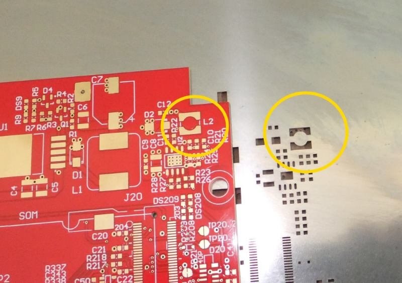
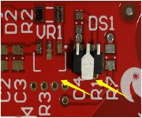
    Today (for the second time) i got e comment from my PCB assembly house that there was a problem with placing an SMT part, as there was no cutout(s) in the soldermask and also no hole(s) is the paste screen.


    First i checked the gerber files i sent to the assembly house, and they were right, for 1 (unique) part there were no holes in the solder and past files for this part.

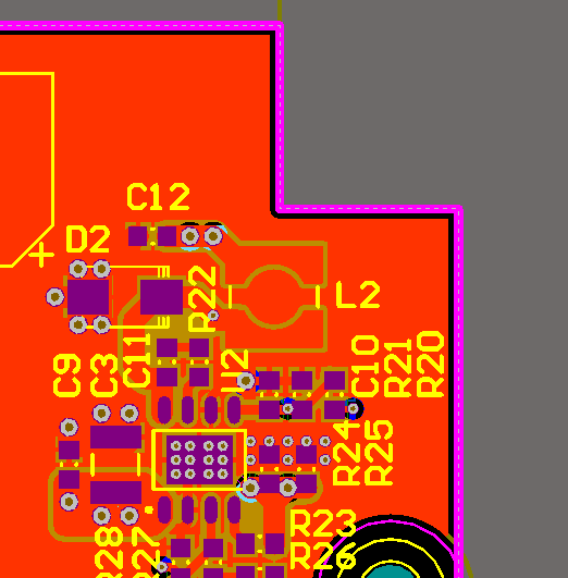
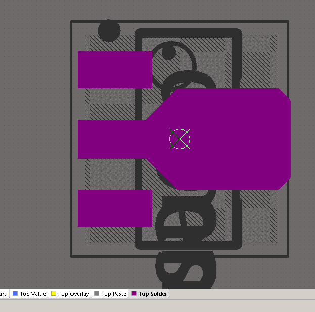
    Then i check my design, same error

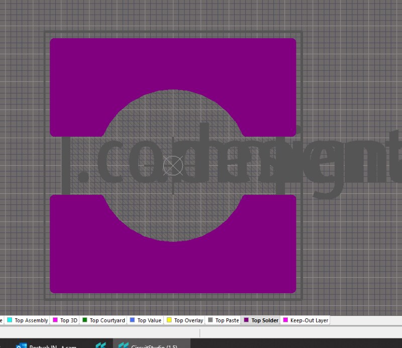
    Then i checked my libary, no problem there, the solder and paste screen where there and drawn correctly


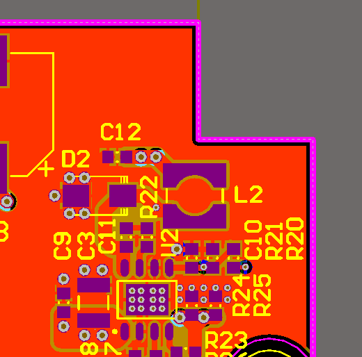
    Reloading the footprint in the design fixed the problem, but....

    At no point in time was an 'incomplete' footprint loaded into my design, either it did not exist yet or it was complete.


    The problem occurred (to me) the first time after a 'respin' of a prototype (red board), some small changes needed to be made for the production series (blue board), but not on the 'problem' part.

    How do i know this, the (red) proto boards have all the layers correct, the updated version (blue board) is 'suddenly' missing solder mask and solder paste information for 1 footprint.


    Images below:

    1) Problem photo sent by assembly house about PCB version 1.1

    2) My reply that the Proto (V1.0) did not have this problem

    3) Found fault in current design files (screen capture)

    4) Screencapture form footprint in library

    5) Screen capture of design files after reloading footprint


    imageimageimageimageimage


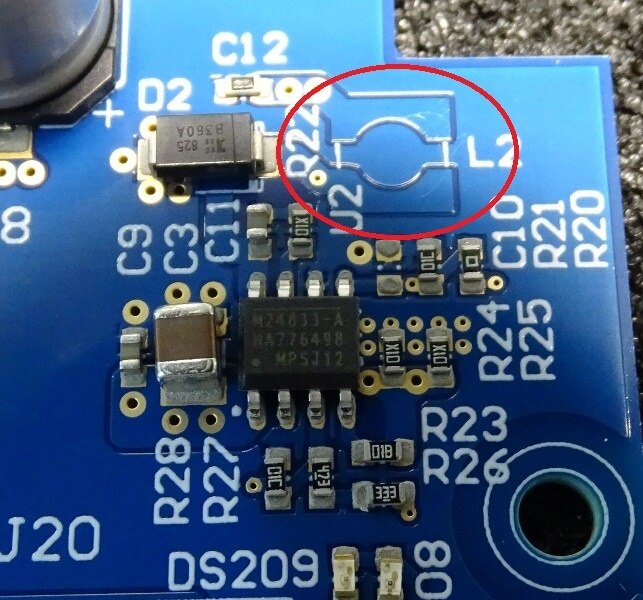
    This second time i got this picture, and again the complete version is in the library:

    imageimage

    I've used this footprint also in other designs before this one, without any problems.


    Can anybody confirm this problem, and can the guys at CS please fix this.


    With kind regards,


    Dexter23

    • Cancel
    • Vote Up 0 Vote Down
    • Cancel
  • Sparkylabs
    0 Sparkylabs over 6 years ago in reply to dexter23

    Just admit defeat, let the money go (£1000 in my case) and move to KiCad, sure it's not perfect but unlike the scam that is CS they actually issue updates. Since i started using it a few months ago 2 updates have come out! the same cannot be said for CS in 2 years!!!!!!!!!!!!!!!!!! and the CS updates are no more than what kiCad put out.


    All CS is, is for Farnell to be able to have thuir own PCB tool like every other man and his dog and for Altiem to get the contact details of a sucker to sell AD to. i have spent £1000 on an advert for Altium designer and a poor advert at that!

    • Cancel
    • Vote Up 0 Vote Down
    • Cancel
Reply
  • Sparkylabs
    0 Sparkylabs over 6 years ago in reply to dexter23

    Just admit defeat, let the money go (£1000 in my case) and move to KiCad, sure it's not perfect but unlike the scam that is CS they actually issue updates. Since i started using it a few months ago 2 updates have come out! the same cannot be said for CS in 2 years!!!!!!!!!!!!!!!!!! and the CS updates are no more than what kiCad put out.


    All CS is, is for Farnell to be able to have thuir own PCB tool like every other man and his dog and for Altiem to get the contact details of a sucker to sell AD to. i have spent £1000 on an advert for Altium designer and a poor advert at that!

    • Cancel
    • Vote Up 0 Vote Down
    • Cancel
Children
No Data
element14 Community

element14 is the first online community specifically for engineers. Connect with your peers and get expert answers to your questions.

  • Members
  • Learn
  • Technologies
  • Challenges & Projects
  • Products
  • Store
  • About Us
  • Feedback & Support
  • FAQs
  • Terms of Use
  • Privacy Policy
  • Legal and Copyright Notices
  • Sitemap
  • Cookies

An Avnet Company © 2026 Premier Farnell Limited. All Rights Reserved.

Premier Farnell Ltd, registered in England and Wales (no 00876412), registered office: Farnell House, Forge Lane, Leeds LS12 2NE.

Follow element14

  • X
  • Facebook
  • linkedin
  • YouTube