element14 Community
element14 Community
    Register Log In
  • Site
  • Search
  • Log In Register
  • Community Hub
    Community Hub
    • What's New on element14
    • Feedback and Support
    • Benefits of Membership
    • Personal Blogs
    • Members Area
    • Achievement Levels
  • Learn
    Learn
    • Ask an Expert
    • eBooks
    • element14 presents
    • Learning Center
    • Tech Spotlight
    • STEM Academy
    • Webinars, Training and Events
    • Learning Groups
  • Technologies
    Technologies
    • 3D Printing
    • FPGA
    • Industrial Automation
    • Internet of Things
    • Power & Energy
    • Sensors
    • Technology Groups
  • Challenges & Projects
    Challenges & Projects
    • Design Challenges
    • element14 presents Projects
    • Project14
    • Arduino Projects
    • Raspberry Pi Projects
    • Project Groups
  • Products
    Products
    • Arduino
    • Avnet & Tria Boards Community
    • Dev Tools
    • Manufacturers
    • Multicomp Pro
    • Product Groups
    • Raspberry Pi
    • RoadTests & Reviews
  • About Us
  • Store
    Store
    • Visit Your Store
    • Choose another store...
      • Europe
      •  Austria (German)
      •  Belgium (Dutch, French)
      •  Bulgaria (Bulgarian)
      •  Czech Republic (Czech)
      •  Denmark (Danish)
      •  Estonia (Estonian)
      •  Finland (Finnish)
      •  France (French)
      •  Germany (German)
      •  Hungary (Hungarian)
      •  Ireland
      •  Israel
      •  Italy (Italian)
      •  Latvia (Latvian)
      •  
      •  Lithuania (Lithuanian)
      •  Netherlands (Dutch)
      •  Norway (Norwegian)
      •  Poland (Polish)
      •  Portugal (Portuguese)
      •  Romania (Romanian)
      •  Russia (Russian)
      •  Slovakia (Slovak)
      •  Slovenia (Slovenian)
      •  Spain (Spanish)
      •  Sweden (Swedish)
      •  Switzerland(German, French)
      •  Turkey (Turkish)
      •  United Kingdom
      • Asia Pacific
      •  Australia
      •  China
      •  Hong Kong
      •  India
      • Japan
      •  Korea (Korean)
      •  Malaysia
      •  New Zealand
      •  Philippines
      •  Singapore
      •  Taiwan
      •  Thailand (Thai)
      • Vietnam
      • Americas
      •  Brazil (Portuguese)
      •  Canada
      •  Mexico (Spanish)
      •  United States
      Can't find the country/region you're looking for? Visit our export site or find a local distributor.
  • Translate
  • Profile
  • Settings
Altium CircuitStudio
  • Products
  • Manufacturers
  • Altium CircuitStudio
  • More
  • Cancel
Altium CircuitStudio
Altium CircuitStudio Forum Split plane is reflected in wrong layer in gerber file
  • Blog
  • Forum
  • Documents
  • Events
  • Polls
  • Members
  • Mentions
  • Sub-Groups
  • Tags
  • More
  • Cancel
  • New
Join Altium CircuitStudio to participate - click to join for free!
Actions
  • Share
  • More
  • Cancel
Forum Thread Details
  • State Not Answered
  • Locked Locked
  • Replies 5 replies
  • Subscribers 88 subscribers
  • Views 1233 views
  • Users 0 members are here
  • frontpage
  • split
  • internal planes
Related
This discussion has been locked.
You can no longer post new replies to this discussion. If you have a question you can start a new discussion

Split plane is reflected in wrong layer in gerber file

vinodkaruvat
vinodkaruvat over 6 years ago

Hi,


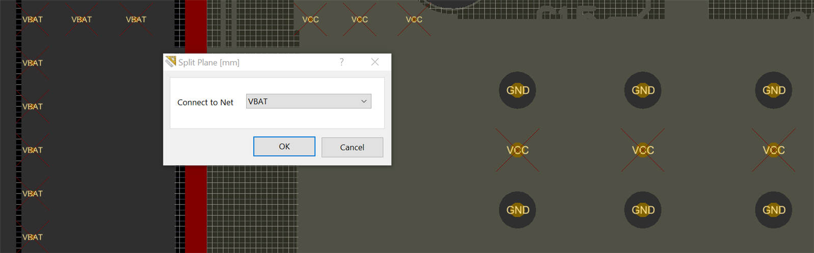
I am designing a 4 layer board - SIgnal1,GND,Vcc and Sig2. In the VCC layer I have 2 planes viz - VBAT and VCC. I have given the split using the line "L" command and drawing a 1mm thick line. The planes seem isolated and look good. Kindly refer the image below. The layer is Internal Plane 2.


image


The Internal Plane 1 just above it looks like -


image


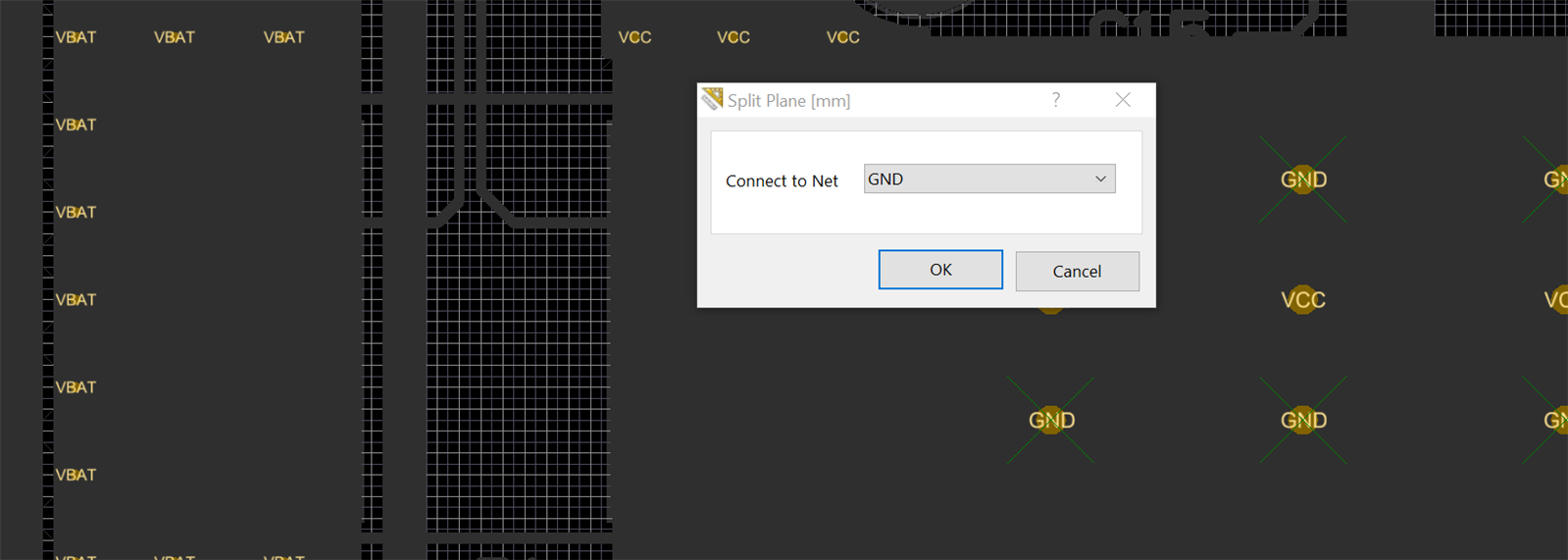
The above is the internal Plane 1  which is GND layer. It looks fine.

Now, I generate the Gerber files and check them on view mate -

GPI - internal plane 2 and GP1 - Internal plane 1. So, GP2 layer is as shown below -


image


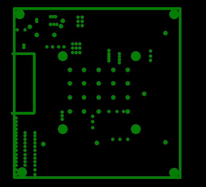
This looks like the GND vias in my design and it also shows a split GND plane. The VCC layer is as shown below -


image


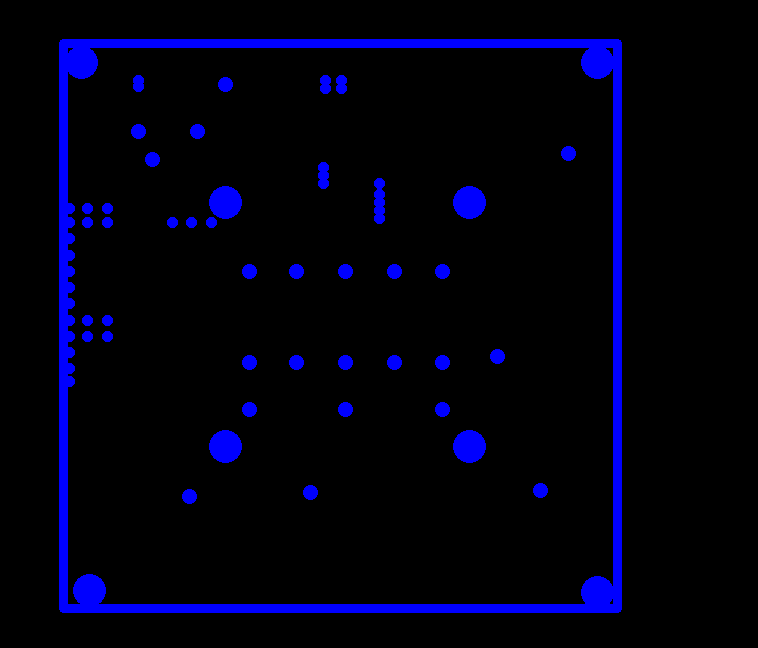
So, there is a complete change in the split plane. How is this so ? Also, when I select loaded preset stack-up, in 4 layer it shows all layers as routing or signal layers. No planar layers. Can you help me out ?


Vinod

  • Cancel
Parents
  • e14softwareuk
    0 e14softwareuk over 6 years ago

    There is a plane layer type in the board stack. If you open the board stack manager use the Add Layer button and select Add Internal Plane. Alternatively you can use normal signal layers and draw a couple of polygons to represent the plane areas.

    • Cancel
    • Vote Up 0 Vote Down
    • Cancel
  • vinodkaruvat
    0 vinodkaruvat over 6 years ago in reply to e14softwareuk

    Thank you for the response. I tried the internal plane approach. But it shows the same thing. The split plane is appearing in the other layer and not the one I intend to place it on. Also, I dont want to go with the 2nd approach that you suggest for now. Have you encountered such a problem before ?


    In Altium, the preloaded stack up for 4 layer is Sig1,Lay1,Lay2,Sig2. It comes correctly so and not Sig1,SIg2,Sig3,Sig4. In the latter we are bending the system to make it a 4 layer. It will work, but if I have denser split planes and nested split planes it will be clumsy.

    • Cancel
    • Vote Up 0 Vote Down
    • Cancel
  • e14softwareuk
    0 e14softwareuk over 6 years ago in reply to vinodkaruvat

    I am confused how the split plane is appearing on the wrong layer. If you have adjusted your board stock to include plane layers then I'm not sure what can go wrong. The predefined layer stacks are just there as examples so it is easy to take the two layer board and add in two internal plane layers to get your 4 layer setup.

    • Cancel
    • Vote Up 0 Vote Down
    • Cancel
  • e14softwareuk
    0 e14softwareuk over 6 years ago in reply to e14softwareuk

    If you want to send me your PCB file to look at so I can better understand then feel free to zip and send the CSPcbDoc file to software@element14.com.

    • Cancel
    • Vote Up 0 Vote Down
    • Cancel
Reply
  • e14softwareuk
    0 e14softwareuk over 6 years ago in reply to e14softwareuk

    If you want to send me your PCB file to look at so I can better understand then feel free to zip and send the CSPcbDoc file to software@element14.com.

    • Cancel
    • Vote Up 0 Vote Down
    • Cancel
Children
  • vinodkaruvat
    0 vinodkaruvat over 6 years ago in reply to e14softwareuk

    Sent

    • Cancel
    • Vote Up 0 Vote Down
    • Cancel
element14 Community

element14 is the first online community specifically for engineers. Connect with your peers and get expert answers to your questions.

  • Members
  • Learn
  • Technologies
  • Challenges & Projects
  • Products
  • Store
  • About Us
  • Feedback & Support
  • FAQs
  • Terms of Use
  • Privacy Policy
  • Legal and Copyright Notices
  • Sitemap
  • Cookies

An Avnet Company © 2026 Premier Farnell Limited. All Rights Reserved.

Premier Farnell Ltd, registered in England and Wales (no 00876412), registered office: Farnell House, Forge Lane, Leeds LS12 2NE.

ICP 备案号 10220084.

Follow element14

  • X
  • Facebook
  • linkedin
  • YouTube