element14 Community
element14 Community
    Register Log In
  • Site
  • Search
  • Log In Register
  • Community Hub
    Community Hub
    • What's New on element14
    • Feedback and Support
    • Benefits of Membership
    • Personal Blogs
    • Members Area
    • Achievement Levels
  • Learn
    Learn
    • Ask an Expert
    • eBooks
    • element14 presents
    • Learning Center
    • Tech Spotlight
    • STEM Academy
    • Webinars, Training and Events
    • Learning Groups
  • Technologies
    Technologies
    • 3D Printing
    • FPGA
    • Industrial Automation
    • Internet of Things
    • Power & Energy
    • Sensors
    • Technology Groups
  • Challenges & Projects
    Challenges & Projects
    • Design Challenges
    • element14 presents Projects
    • Project14
    • Arduino Projects
    • Raspberry Pi Projects
    • Project Groups
  • Products
    Products
    • Arduino
    • Avnet Boards Community
    • Dev Tools
    • Manufacturers
    • Multicomp Pro
    • Product Groups
    • Raspberry Pi
    • RoadTests & Reviews
  • Store
    Store
    • Visit Your Store
    • Choose another store...
      • Europe
      •  Austria (German)
      •  Belgium (Dutch, French)
      •  Bulgaria (Bulgarian)
      •  Czech Republic (Czech)
      •  Denmark (Danish)
      •  Estonia (Estonian)
      •  Finland (Finnish)
      •  France (French)
      •  Germany (German)
      •  Hungary (Hungarian)
      •  Ireland
      •  Israel
      •  Italy (Italian)
      •  Latvia (Latvian)
      •  
      •  Lithuania (Lithuanian)
      •  Netherlands (Dutch)
      •  Norway (Norwegian)
      •  Poland (Polish)
      •  Portugal (Portuguese)
      •  Romania (Romanian)
      •  Russia (Russian)
      •  Slovakia (Slovak)
      •  Slovenia (Slovenian)
      •  Spain (Spanish)
      •  Sweden (Swedish)
      •  Switzerland(German, French)
      •  Turkey (Turkish)
      •  United Kingdom
      • Asia Pacific
      •  Australia
      •  China
      •  Hong Kong
      •  India
      •  Korea (Korean)
      •  Malaysia
      •  New Zealand
      •  Philippines
      •  Singapore
      •  Taiwan
      •  Thailand (Thai)
      • Americas
      •  Brazil (Portuguese)
      •  Canada
      •  Mexico (Spanish)
      •  United States
      Can't find the country/region you're looking for? Visit our export site or find a local distributor.
  • Translate
  • Profile
  • Settings
Altium CircuitStudio
  • Products
  • Manufacturers
  • Altium CircuitStudio
  • More
  • Cancel
Altium CircuitStudio
Altium CircuitStudio Forum How to set routing vias be covered with mask? Always.
  • Blog
  • Forum
  • Documents
  • Events
  • Polls
  • Members
  • Mentions
  • Sub-Groups
  • Tags
  • More
  • Cancel
  • New
Join Altium CircuitStudio to participate - click to join for free!
Actions
  • Share
  • More
  • Cancel
Forum Thread Details
  • State Not Answered
  • Locked Locked
  • Replies 5 replies
  • Subscribers 87 subscribers
  • Views 3295 views
  • Users 0 members are here
  • routung vias
  • solder mask
  • vias
Related
This discussion has been locked.
You can no longer post new replies to this discussion. If you have a question you can start a new discussion

How to set routing vias be covered with mask? Always.

olemi
olemi over 6 years ago

This doc describes the process for non-routing vias:

http://documentation.circuitstudio.com/display/CSTU/PCB_Dlg-Via((Via))_CS


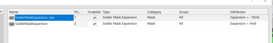
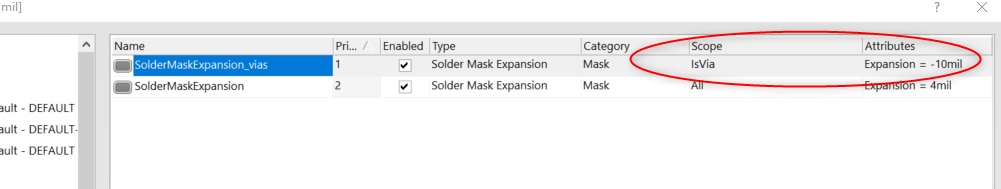
"PCB rules > Routing Via Style" doesn't have Solder Mask Expansion option.


"PCB rules > Solder Mask Expansion" doesn't have vias for the object.


How?

  • Cancel
  • tarribred61
    0 tarribred61 over 6 years ago

    I suspect you won't be satisfied but here is a complicated way to do it using rules.  For a simpler way see my follow-up post below about using PCB filters. The rules method would change expansion rules on ALL vias but it may be possible to change to be more specific with more effort.

    If you really need to have good control of the rules then you may need to pay for full Altium Designer which has very good editors and logic testing for complex logical statements. Or hope someone will build a separate utility app to manipulate the rule text.


    Otherwise, you can manually take control in a painful process.  Hopefully, this will give some readers a clue as to how this works and they can devise a better method.  (Or it will scare them off.)


    Open the PCB Rules and Constraints Editor (Home > Design Rules).

    Go to Mask>Solder Mask Expansion and then right mouse click and add New Rule; give it a name like SolderMaskExpansion_vias. Click Apply button.


    Observe the column that says Scope.  Is should say "All" or "(All)" for a value.  Change the attributes to a large negative value if you want to tent fully or to whatever you want it to be.  Here I have changed mine to be -10mil.

    image


    Right mouse click anywhere in the navigation pane for the rules tree and choose Export Rules.

    Pick Solder Mask Expansion rule to select it for export; press OK.

    Choose a place to export the RUL file to rather than the default (maybe a folder named CS_Rule_Sandbox or something.  Name the file something appropriate rather than the generic default.

    Use your favorite text editor to open the filename.RUL file.


    For example, this is what I get from the default as the default.

    SELECTION=FALSE|LAYER=TOP|LOCKED=FALSE|POLYGONOUTLINE=FALSE|USERROUTED=TRUE|UNIONINDEX=0|UNIQUEID=ICMNQFCH|RULEKIND=SolderMaskExpansion|NETSCOPE=AnyNet|LAYERKIND=SameLayer|SCOPE1EXPRESSION=All|SCOPE2EXPRESSION=All|NAME=SolderMaskExpansion|ENABLED=TRUE|PRIORITY=2|COMMENT= |DEFINEDBYLOGICALDOCUMENT=FALSE|EXPANSION=4mil


    If you add another rule then you would get more entries.  Since, we added another rule above I get the following in my editor.  It isn't in a pretty and human readable format but it is in text.

    SELECTION=FALSE|LAYER=UNKNOWN|LOCKED=FALSE|POLYGONOUTLINE=FALSE|USERROUTED=TRUE|UNIONINDEX=0|UNIQUEID=AATYVYYQ|RULEKIND=SolderMaskExpansion|NETSCOPE=AnyNet|LAYERKIND=SameLayer|SCOPE1EXPRESSION=All|SCOPE2EXPRESSION=All|NAME=SolderMaskExpansion_vias|ENABLED=TRUE|PRIORITY=1|COMMENT= |DEFINEDBYLOGICALDOCUMENT=FALSE|EXPANSION=-10mil

    SELECTION=FALSE|LAYER=TOP|LOCKED=FALSE|POLYGONOUTLINE=FALSE|USERROUTED=TRUE|UNIONINDEX=0|UNIQUEID=ICMNQFCH|RULEKIND=SolderMaskExpansion|NETSCOPE=AnyNet|LAYERKIND=SameLayer|SCOPE1EXPRESSION=All|SCOPE2EXPRESSION=All|NAME=SolderMaskExpansion|ENABLED=TRUE|PRIORITY=2|COMMENT= |DEFINEDBYLOGICALDOCUMENT=FALSE|EXPANSION=4mil


    You can edit the rule scope. Above it would be SCOPE1EXPRESSION=All. Change text All to be IsVia.  You'll also see a SCOPE2EXPRESSION.  This is what AD uses and I don't know if CS will ignore it or use it also.  This can perhaps experimented with it in future.


    To make more complex rules you would need to read and understand Altium's rule expressions and how to use AND and OR and parenthesis.


    So now my rule expressions are:

    SELECTION=FALSE|LAYER=UNKNOWN|LOCKED=FALSE|POLYGONOUTLINE=FALSE|USERROUTED=TRUE|UNIONINDEX=0|UNIQUEID=AATYVYYQ|RULEKIND=SolderMaskExpansion|NETSCOPE=AnyNet|LAYERKIND=SameLayer|SCOPE1EXPRESSION=IsVia|SCOPE2EXPRESSION=All|NAME=SolderMaskExpansion_vias|ENABLED=TRUE|PRIORITY=1|COMMENT= |DEFINEDBYLOGICALDOCUMENT=FALSE|EXPANSION=-10mil

    SELECTION=FALSE|LAYER=TOP|LOCKED=FALSE|POLYGONOUTLINE=FALSE|USERROUTED=TRUE|UNIONINDEX=0|UNIQUEID=ICMNQFCH|RULEKIND=SolderMaskExpansion|NETSCOPE=AnyNet|LAYERKIND=SameLayer|SCOPE1EXPRESSION=All|SCOPE2EXPRESSION=All|NAME=SolderMaskExpansion|ENABLED=TRUE|PRIORITY=2|COMMENT= |DEFINEDBYLOGICALDOCUMENT=FALSE|EXPANSION=4mil


    Go back to CS and right mouse click in the rules tree and choose Import Rules.  Select the Solder Mask Expansion rule type and press OK. Navigate and select the file you just edited and press Open.  When it asks to clear existing rules prior to import is may be safest to click No.


    You should see the scope of the rule change now to IsVia.

    image

    Click Apply and then OK to close the Rules editor.


    If you view the PCB in 3D you should see the vias now have solder mask encroached with a negative expansion.


    If you need to, you should be able to put a large negative value in the via expansion rule to fully tent.


    Good luck.

    • Cancel
    • Vote Up 0 Vote Down
    • Cancel
  • tarribred61
    0 tarribred61 over 6 years ago in reply to tarribred61

    Actually, the simpler method to select vias and globally change them, you might also try to it with the Object Inspector and or PCB Filter menus.


    You should be able to use those to just select the vias and then change them.


    Use PCB filter to just highlight the vias.  Then drag your mouse around them to select them.  Then use the Object Inspector to see the properties.  Edit to change tenting.


    Basically this is discussed on the following link

    Altium CircuitStudio Knowledge Base

    and specifically here Tenting All Vias

    • Cancel
    • Vote Up 0 Vote Down
    • Cancel
  • olemi
    0 olemi over 6 years ago in reply to tarribred61

    Was it a joke? image

    Sure, I won't!

    I already regretted several times that I decided to move from 15-years-old-never-updated Layout 16.2 which happened to had everything expect 3D and multi-undo.


    I really surprised that modern CAD doesn't have many "MUSTs" and each time there is a headache-like workaround instead of a really simple solution that even 15 years old CADs have.


    >>Actually, the simpler method

    I would definitely agree with "simpler" in compare with the first post image if it would really work. There is no way to set a negative tenting for vias in the Object Inspector. ...And guys (from CS)... is it really modern user-friendly approach to set a negative value for "no open mask" instead of having a separate checkbox just for that? The same for paste.


    Also, selecting "all" vias is not what I need. Some non-routing vias should be with mask. Filters are useless here too.


    As for the workaround in a form of the Object Inspector, which seems is a way to go for many workarounds in CS I should mention it doesn't have all fields to edit that individual property windows have (just another example, but for the same subject: editing footprints, e.g. 64 pins of MCU for mask expansion value and some other properties).


    • Cancel
    • Vote Up 0 Vote Down
    • Cancel
  • ryanjenson90
    0 ryanjenson90 over 6 years ago in reply to tarribred61

    thank you

    i guess this is far better option. https://techyhost.com/voice-chat-software/ is the best way to do this !

    its even simpler.

    • Cancel
    • Vote Up 0 Vote Down
    • Cancel
  • olemi
    0 olemi over 6 years ago in reply to ryanjenson90

    image

    Could you please clarify where did you find here how to keep mask closed on, let's simplify, all selected vias?

    • Cancel
    • Vote Up 0 Vote Down
    • Cancel
element14 Community

element14 is the first online community specifically for engineers. Connect with your peers and get expert answers to your questions.

  • Members
  • Learn
  • Technologies
  • Challenges & Projects
  • Products
  • Store
  • About Us
  • Feedback & Support
  • FAQs
  • Terms of Use
  • Privacy Policy
  • Legal and Copyright Notices
  • Sitemap
  • Cookies

An Avnet Company © 2025 Premier Farnell Limited. All Rights Reserved.

Premier Farnell Ltd, registered in England and Wales (no 00876412), registered office: Farnell House, Forge Lane, Leeds LS12 2NE.

ICP 备案号 10220084.

Follow element14

  • X
  • Facebook
  • linkedin
  • YouTube