Hi. Not sure if the diagram is showing pads or vias, however you can achieve a solder mask clearance rather than tented quite easily. Bring up the properties dialog for the via/pad and make sure Force Tenting Top/Bottom options are not checked. Next if you have specified a Solder Mask Expansion Value this may need adjusting, the larger the number the more clearance around the hole. Finally if the previous have not fixed it then check the design rules where a Solder Mask Expansion rule may need adjusting.
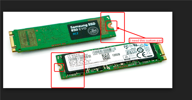
The basics of making a custom pad are to draw the shape(s) you want on the copper layer(s) and then copy the same shapes to the solder mask layer. Any shapes you draw on the solder mask layer will make openings. It looks like you are not putting solder paste on the pads so you leave the solder paste layer alone. If the pads are both the same on top and bottom then you only need to draw this as a surface mount component and place it on both sides of the board. If you have vias connecting both sides, or want to electrically connect top and bottom pads, then you can draw this as a single component and put the shapes on top and bottom copper and top and bottom solder mask and add the vias. Or you could keep it as a single layer pad only and place one top and bottom then add stitching vias to connect at the PCB level. The link sent by Peter Barnard says something about how to assign a net name to the pads.
I'd suggest making the pad in the PCB library and then placing on your board. You can create a corresponding schematic library part that looks something like a simple test point or mounting hole and links to the PCB lib part with the custom footprint.
I don't think CircuitStudio will let you convert selected lines into a polygon (Altium Designer does). So instead you can place arcs and lines on a layer and then use them as guides to free hand draw the shape of the pad you want.
I think you can do that in the PCB level but not at the PCB library level. You might be able to do it on the PCB level and then cut and paste a shape into the PCB library though.