


8 Tips and tricks for EMI migration on your design
Author: Dheeraj Jain, Technology Strategist; Jenna Cummins
1. Earlier is better
Don’t underestimate EMI issues, as they can cost a lot of time and money to fix. The earlier you pay attention to possible EMI issues, the faster and cheaper your product release will be. Waiting until the last minute to address potential issues could cause redesign of the board or result in an expensive solution to fix the EMI.
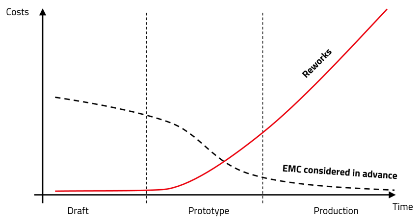
Figure 1. Costs and time of design process with and without considering EMC in advance.
2. Keep the inductor close to the IC
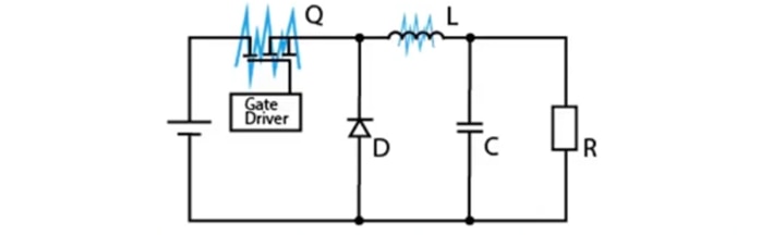
Figure 2. Importance of design layout.
A high current loop with fast di/dt is formed by the input capacitor, the switch, and diode which is a H-field loop antenna. The smallest parasitic inductance and capacitance generate high frequency ringing. This is the main cause of differential mode noise. A low ESR capacitor and tight layout minimizes the radiated field from conduction in this loop.
3. Orient the inductor to your advantage
There is a hot node at the connection of the MOSFET source terminal, the cathode of the diode and the inductor. This node has high dv/dt creating an undesirable E-field antenna. Parasitic capacitances allow RF currents to flow to ground causing common mode noise. Again, this area must be minimized. The inductor’s dot mark indicates the start of the winding, the inner most part which should be connected to this node to minimize the area, the parasitic capacitance and to partially shield it.
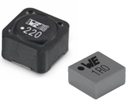
Figure 3. Example of Würth Elektronik inductors with dot marks where winding begins.
4. Distribution of Ground (aka GND)
Be careful how your system is grounded. Each part of the system is supposed to be grounded separately. When any point in the system is connected with more than one path of ground, we might create a ground loop, which can create the perfect way for disturbance to travel through the system and affect the entire design. When using long cables to connect different devices, this might turn into a radiated emissions problem. A lot of engineers have to deal with EMC problems due to a lacking ground concept. The underlying coupling mechanism is called “impedance coupling“. We want to have as little as possible of this shared impedance in the Ground and VCC lines. That‘s why we usually distribute ground in a star topology. This not only helps with emissions, but with immunity as well!
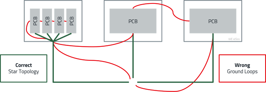
Figure 4. Correct and incorrect grounding examples.
5. Ground Reference @ IC Pins
In the bad example below, we see two circuits routed via the IC pin that could cause unwanted coupling between them. This can be improved by using separate current paths in a star shape and the addition of multiple vias to create short loops.
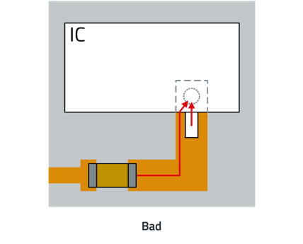
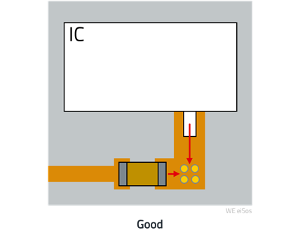
Figure 5. Routing circuits to reduce coupling.
6. Reduce impedance to ground
Every mm of pcb trace adds up 1 nH of parasitic capacitance. That may not seem like much, but it can be significant when running the design at high frequency as it acts as an antenna.
Long ground paths lead to increased parasitic inductances (1nH / mm). High-frequency clocked ICs cause interference voltages on the ground due to their load currents. For a short low-inductance connection, each pin receives its own VIA to the ground plane.
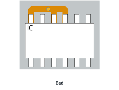
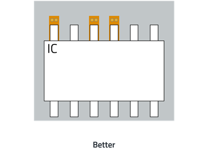
Figure 6. Reducing impedance to ground in a design.
7. Distance between GND and VCC layer.
Sandwiching the Signal layer between GND and VCC leads to capacitive coupling. Higher interference signal levels on the power supply couple to the signal position. Ripple voltage, load jumps, etc. generate interference voltages on the signal layer. Positioning GND between the Signal layer and VCC acts as a shield and the high frequency noise is directly diverted to ground. (Note that GND requires low impedance connection.) You can reduce the distance between VCC and GND to 100µm or less to tightly couple these layers.
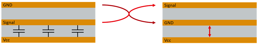
Figure 7. Placing GND between the Signal layer and VCC.
8. Diverting disturbances to earth
The cable is a very good antenna for common mode noise – both for receiving and transmitting!
Both ESD and Common Mode noise revert to PE/ Chassis Ground. Connecting your PCB to chassis ground is very good idea to give those disturbances a clear way back. However, you shouldn‘t just place this connection anywhere; placing it far away from their origin gives both the ESD and CM current a chance to influence and damage your application. That’s why we place these steel spacers as close to the I/O ports as possible. We can place a ceramic safety Y-Cap to have a low impedance RF coupling to chassis while maintaining DC isolation.
For CM emissions, that will act as a short and keep the common mode loop small. The incoming CM current and the ESD are both diverted away from the electronics. Take care to make all these connections low impedance.
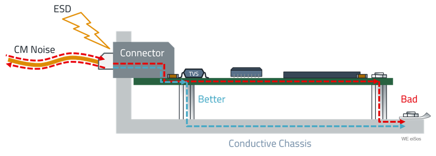
Figure 8. Good and bad examples for connecting your PCB to chassis ground.

