Application Note
Coaxial PCB Connector
PCB-Transmission Line Design Guide
ANE012 BY OLAN TSAI
1 Introduction
The function of a RF (Radio Frequency) transmission line is a directing RF signal from a source to a load with minimal loss and distortion. Impedance plays an important role in signal transmission. Even if the trace impedance already matches, adding a connector can cause an impedance mismatch and thus signal distortions due to reflections. The purpose of this application note is to outline methods for improving signal transmission when a connector is added on a PCB.
1.1. Impedance
Impedance matching determines the transmission line performance. Characteristic impedance of a standard transmission line is expressed as:
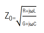
According to the formula above, the main factors include: R(resistance per meter), L(inductance per meter), C(capacitance per meter), G(conductance per meter), and last but not least the angular frequency ω.
1.2. Types of RF Transmission line on PCB
Applications define the selection of suitable types of transmission lines:
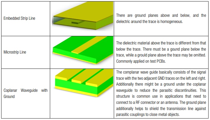
Figures 1 to 3 – Types of RF transmission lines
2 RF Transimission Line Design Parameter
The coplanar waveguide with ground is typically found on PCBs with a coaxial connector; therefore, we use this RF transmission line as example.
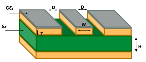
Figure 4: Coplanar waveguide
Factors that determine the PCB transmission-line characteristic impedance are:
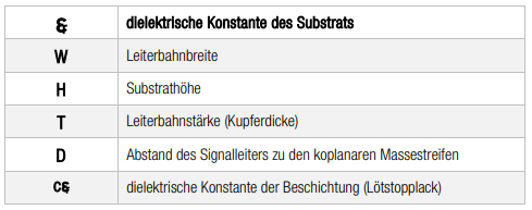
Table 1: Influencing factors on characteristic impedance
Suggested design flow for a RF transmission line is as follows:
a) Select the PCB substrate.
- For example: FR1, FR4, CEM1…etc.
b) Define the PCB’s properties:
- εr: Substrate dielectric constant
- H: Substrate height
- T: Trace thickness
- cεr: Coating dielectric constant
c) Control and adjust the value of W and D to reach the required characteristic impedance.
d) If step (c) cannot be achieved, please return to step (b) to select a different substrate height and trace thickness. Return to (a) when the newly selected properties in step (b) still cannot achieve the desired impedance.
3 Relationship for Each Parameter with Characteristic Impedance
It is important to understand how each factor influences the transmission line. Each paragraph below indicates how the characteristic impedance will change when only one of these factors is adjusted.
3.1. εr - Substrate Dielectric Constant
Many different types of materials can be used as PCB substrate. Each substrate has its own dielectric constant. The user needs to be aware of “PCB Material Dielectric Constant” given by manufacturers.
On the other hand, material dielectric constant will vary not only between vendors but with the frequency, too.
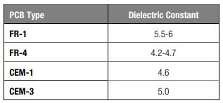
Table 2: Dielectric constants for common PCB materials
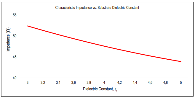
Figure 5: This figure shows impedance (Z0) is inversely proportional to dielectric constant (εr)
3.2. W - Trace Width
For trace width design, the user needs to consider four things:
1) Narrow traces are more difficult to control
2) Wider traces need more space on the PCB.
3) Actual trace width may not be as designed due to manufacturing tolerance.
4) Because the wave impedance and the height of the dielectric material is fixed, these parameters will decide the trace width.
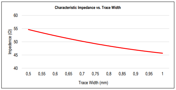
Figure 6: This figure shows impedance (Z0) is roughly inverse-proportional to trace width
3.3. H - Substrate Height
The substrate height is the distance between the ground and signal layer of a PCB. The characteristic impedance reduces if the copper layers are closer together and the other parameters are fixed. To maintain the impedance of the trace, the trace width can be reduced. This in turn saves space on PCB. But please note, if narrower tracks are used, the tolerance of the impedance will be greater due to the undercutting during manufacturing process!
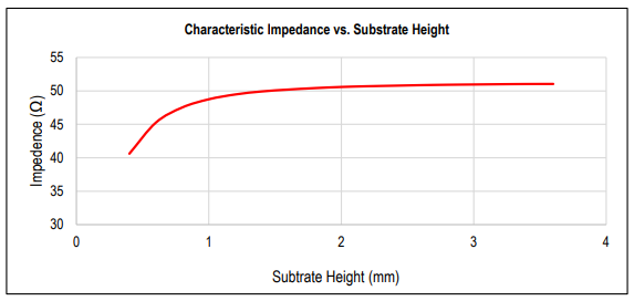
Figure 7: Impedance (Z0) increases more slowly when substrate height is at specific distance
3.4. T - Trace Thickness (height of the copper layer)
Copper is commonly used as the PCB metal layer in layer heights of 0.5 oz/ft2 (0.017mm), 1 oz/ft2 (0.035mm) or 2 oz/ft2 (0.070mm). The characteristic impedance reduces, if the Cu copper thickness (height of the copper layer) is increased.
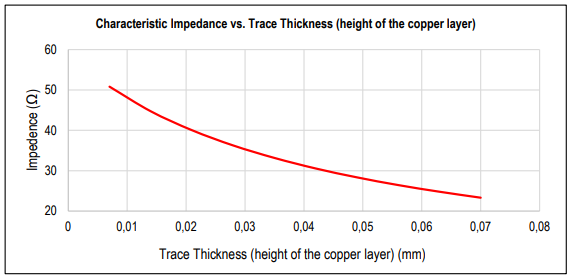
Figure 8: Impedance (Z0) is roughly inverse-proportional to the trace thickness (height of the copper layer)
3.5. D - Distance between Trace and Coplanar Ground
This factor is very sensitive. It can influence the impedance by 1~2 Ω with only 0.01 mm variation, hence the PCB manufacturing precision needs to be checked when doing this adjustment.
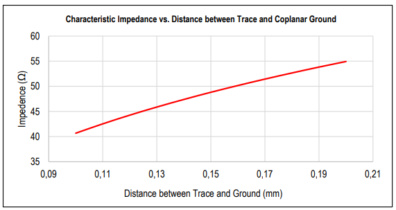
Figure 9: Impedance (Z0) is roughly proportional to the distance between trace and coplanar ground
3.6. Cεr - Coating Dielectric Constant
The coating material’s permittivity also has an influence on characteristic impedance. It should be considered early in the design stage in order to avoid deviation from calculated values.
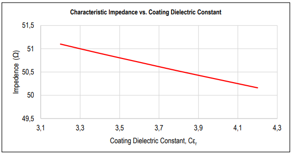
Figure 10: Impedance (Z0) is roughly inverse-proportional to the coating dielectric constant
4 Connector Pin Contact to PCB
When the connector center pin is connected to the PCB trace, it adds a certain height on top of the PCB trace due to its defined size. This height creates a discontinuity and should be fixed by adjusting the trace width on PCB.
4.1. End Launch Round Post Pin
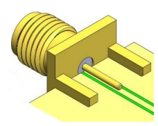
Figure 11: Round post connectors have a larger center pin which creates significant discontinuity after soldering.
To match with the “microstrip line”, the trace width needs to be changed to fit with the round post pin.
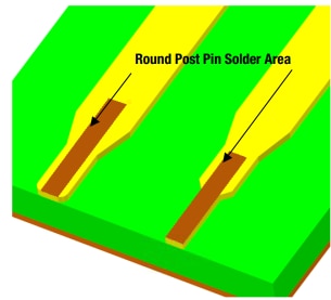
Figure 12: Example of modify the trace shape to improve matching.
If the impedance value is too low from the ideal matching impedance, try to use the shape shown on the left side of figure 12. The trace width near the connector center pin must be reduced. Making the trace width narrower at the end will make a better match.
For a coplanar waveguide, the impedance value can be increased by increasing the distance between the trace and its coplanar ground (GND). It is also possible to reach the ideal impedance by reducing the width of signal trace.
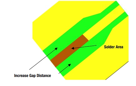
Figure 13: Example of increase the gap distance to improve impedance matching.
4.2. End Launch Flat Tab Pin
This connector usually has a smaller center pin and has less influence on impedance discontinuity after soldering. When the flat pin makes the impedance lower, it can be raised by reducing the width of trace or increasing the gap distance between trace and its coplanar ground (GND).
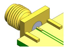
Figure 14: End Launch Flat Tab Pin
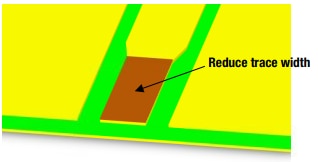
Figure 15: Example of reduced trace width to improve impedance matching
4.3. THT Pin & SMT Pin
THT and SMT connectors are more difficult to reach the ideal match. This is often caused by the gap after the connector is soldered on to PCB. The gap will make the impedance value higher.
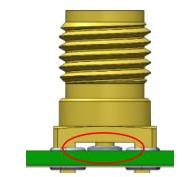
Figure 16: Gap between PCB and connector
Furthermore, THT and SMT connectors that are perpendicular to the trace on PCB which make the impedance lower. For THT center pin, the extended connector legs will make the impedance value lower. Impedance discontinuity occurs over a very short distance for THT and SMT connectors, which is more difficult to fix by adjusting the traces on PCB.
THT and SMT connectors are normally not used in very high-frequency products, because of impedance matching issues.
How the signal is routed from a THT connector changes the impedance.
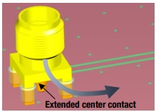
Figure 17: Signal route: Connector interface PCB trace
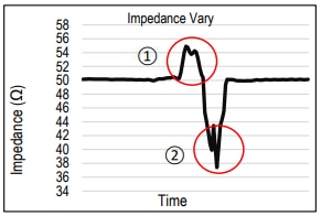
Figure 18: Impedance in time domain
1. Gaps make the impedance higher
2. Vertical area and extended center contact make the impedance lower
How the signal is routed from a SMT connector changes the impedance.
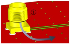
Figure 19: Signal route: Connector interface PCB trace
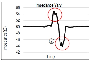
Figure 20: Impedance in time domain
1. Gaps make impedance higher
2. Vertical area makes impedance lower
Figures 17 to 20 show the impact of the connector construction and its connections to the PCB in the time domain. It was measured with a time domain reflectometer (TDR) which determines the impedance of the measured construction by observing the reflected waveform. The change of the impedance over time can be recalculated via εr to the point of reflection.
How to Improve:
1) Gaps make the impedance higher: Use solder paste to fill up gaps to improve the impedance.
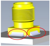
Figure 21: Use solder paste to fill up gaps
2) Vertical area makes the impedance lower: Increase the gap between the contact pin and the GND to reduce the impedance
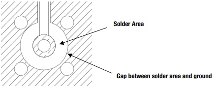
Figure 22: Layout modification to improve the matching
3) Extended connector legs make the impedance lower: Extended connector legs not only make the impedance value lower, they might also cause an antenna effect. Methods to solve this are:
- Select the connector pin length to better match PCB thickness.
- Cut long legs for a significant improvement.
5 Other factors affecting the impedance
Following a few points that will influence the transmission line impedance when making a PCB:
5.1. PCB cut Line(End Launch Coaxial Connector Issue)
PCB routing tolerances occur during PCB production. If the ground layer does not extend to end of the PCB, the PCB routing tolerance might cause a gap between PCB and the connector which will cause an impedance discontinuity.

Figure 23: Ground not extended to end of the PCB
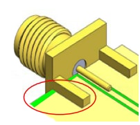
Figure 24: After soldering the connector, a gap exist without ground
We would suggest extending the ground layer on the connector side to the edge. If PCB routing tolerances issues occur, there will be no gap after the connector is soldered to the PCB.

Figure 25: Extended ground to the end of the PCB
5.2. PCB Trim Line (End Launch Edge Card Coaxial Connector Issue)
The PCB routing cannot cut a sharp right angle and the round corners might cause a gap between the connector and the PCB. Because they could not meet closely this causes an impedance discontinuity (figure 25). To fix this, we suggest using Ø0.6-2 mm relief holes in the corners in order to remove the corner radius, as displayed in figure 26.
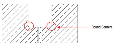
Figure 25: Round corners cause poor mechanical matching of the connector
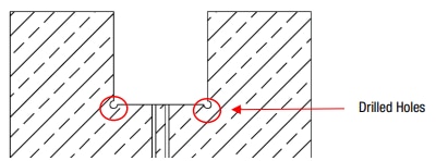
Figure 26: Additional holes improve the fit of the connector
5.3. End Launch Connector and the Backside of a PCB
When an end launch connector is placed on a PCB, if the copper layer is not extended to the PCB edge, there would be a small gap in between. Use of solder paste to fill up the gap can be helpful to impedance control (figure 27).
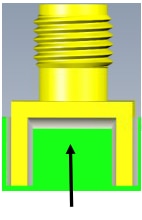
Figure 27: Use solder paste to fill up the gap
5.4. Via Hole
When using a coplanar waveguide design, it is suggested to add some via holes to the coplanar GND surrounding the trace, as shown in figure 28. The via holes connect the upper traces and the bottom layer which is the ground layer. Depending on the highest signal frequency, the vias should have a distance of not more then 2 – 4 mm to make sure, that the coplanar GND-traces keep their GND potential
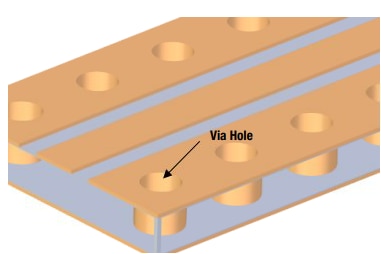
Figure 28: Via implementation from the coplanar ground traces to the ground (GND) layer
6 Simulation Examples
PCB End Launch Jack Round Post for 1.6mm PCB
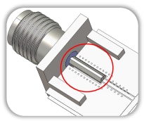
Figure 29: Original Design
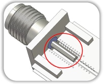
Figure 30: Matching Design
Increase the gap between trace and ground to increase the impedance and reach impedance matching
Result of TDR measurement (Original Design):
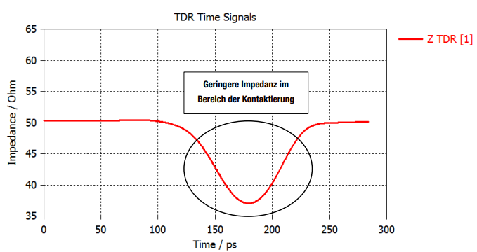
Figure 31: Result of TDR measurement (Original Design)
Result of TDR measurement (Matching Design):
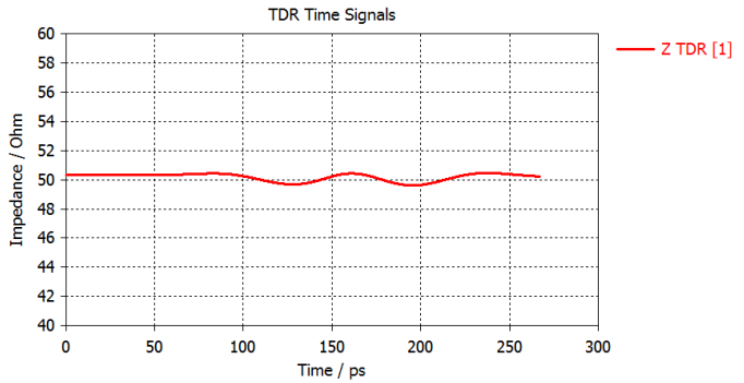
Figure 32: Result of TDR measurement (Matching-Design)
Result of S-Parameter measurement (Original Design):
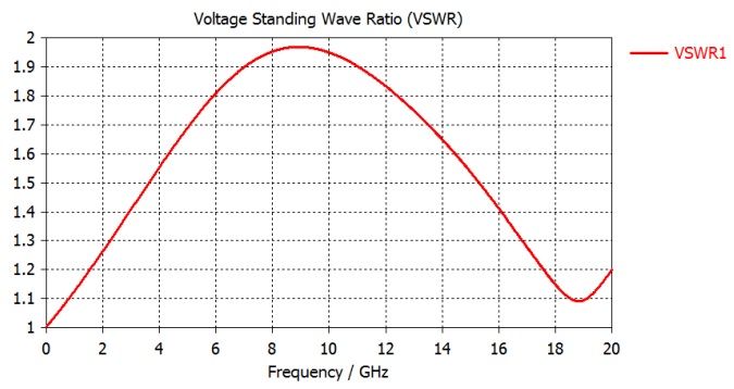
Figure 33: Result of S-Parameter – VSWR measurement (Original Design)
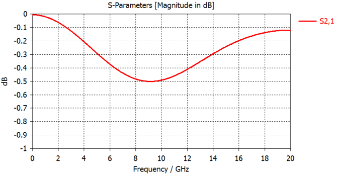
Figure 34: Result of S-Parameter - Return Loss measurement (Original Design)
Result of S-Parameter measurement (Matching Design):
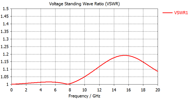
Figure 35: Result of S-Parameter - VSWR measurement (Matching Design)
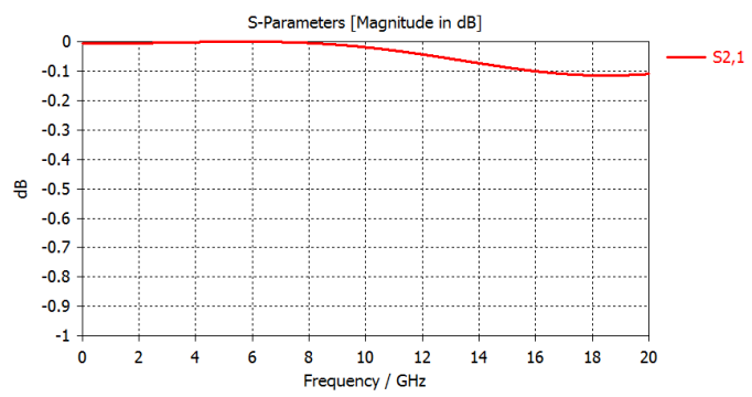
Figure 36: Result of S-Parameter – Return Loss measurement (Matching Design)
7 Conclusion
Simulation software is very useful when designing a transmission line, Software like AppCAD, for example, can simulate transmission lines with different factors. Using the result from AppCAD, software like HFSS can provide full-wave simulations, including both connector and PCB. Overall, using simulation software can save a lot of time.
Knowing the preciseness of PCB production will also help the user design a transmission line because most transmission lines are very narrow. If the PCB has wide tolerances from production, the user’s test results will have huge difference compared to software simulations. Sometimes, roughness of copper layer is a factor that affects impedance of transmission line.
The quality of a transmission line is one part of transmission quality in a product. Users now should understand how to enhance transmission line quality after reading through these suggestions.
IMPORTANT NOTICE
The Application Note is based on our knowledge and experience of typical requirements concerning these areas. It serves as general guidance and should not be construed as a commitment for the suitability for customer applications by Würth Elektronik eiSos GmbH & Co. KG. The information in the Application Note is subject to change without notice. This document and parts thereof must not be reproduced or copied without written permission, and contents thereof must not be imparted to a third party nor be used for any unauthorized purpose. Würth Elektronik eiSos GmbH & Co. KG and its subsidiaries and affiliates (WE) are not liable for application assistance of any kind. Customers may use WE’s assistance and product recommendations for their applications and design. The responsibility for the applicability and use of WE Products in a particular customer design is always solely within the authority of the customer. Due to this fact it is up to the customer to evaluate and investigate, where appropriate, and decide whether the device with the specific product characteristics described in the product specification is valid and suitable for the respective customer application or not. The technical specifications are stated in the current data sheet of the products. Therefore the customers shall use the data sheets and are cautioned to verify that data sheets are current. The current data sheets can be downloaded at www.we-online.com. Customers shall strictly observe any product-specific notes, cautions and warnings. WE reserves the right to make corrections, modifications, enhancements, improvements, and other changes to its products and services. WE DOES NOT WARRANT OR REPRESENT THAT ANY LICENSE, EITHER EXPRESS OR IMPLIED, IS GRANTED UNDER ANY PATENT RIGHT, COPYRIGHT, MASK WORK RIGHT, OR OTHER INTELLECTUAL PROPERTY RIGHT RELATING TO ANY COMBINATION, MACHINE, OR PROCESS IN WHICH WE PRODUCTS OR SERVICES ARE USED. INFORMATION PUBLISHED BY WE REGARDING THIRD-PARTY PRODUCTS OR SERVICES DOES NOT CONSTITUTE A LICENSE FROM WE TO USE SUCH PRODUCTS OR SERVICES OR A WARRANTY OR ENDORSEMENT THEREOF. WE products are not authorized for use in safety-critical applications, or where a failure of the product is reasonably expected to cause severe personal injury or death. Moreover, WE products are neither designed nor intended for use in areas such as military, aerospace, aviation, nuclear control, submarine, transportation (automotive control, train control, ship control), transportation signal, disaster prevention, medical, public information network etc. Customers shall inform WE about the intent of such usage before design-in stage. In certain customer applications requiring a very high level of safety and in which the malfunction or failure of an electronic component could endanger human life or health, customers must ensure that they have all necessary expertise in the safety and regulatory ramifications of their applications. Customers acknowledge and agree that they are solely responsible for all legal, regulatory and safety-related requirements concerning their products and any use of WE products in such safetycritical applications, notwithstanding any applications-related information or support that may be provided by WE. CUSTOMERS SHALL INDEMNIFY WE AGAINST ANY DAMAGES ARISING OUT OF THE USE OF WE PRODUCTS IN SUCH SAFETY-CRITICAL APPLICATIONS.
DIRECT LINK
USEFUL LINKS:
Application Notes : https://we-online.com/en/support/knowledge/application-notes
Services: https://we-online.com/en/products/components/service
Contact : https://we-online.com/en/support/contact
CONTACT INFORMATION
Würth Elektronik eiSos GmbH & Co. KG
Max-Eyth-Str. 1, 74638 Waldenburg, Germany
Tel.: +49 (0) 7942 / 945 – 0
Email: appnotes@we-online.de

