Application Note
Understanding Phototransistor Optocouplers
ANO007 by Eleazar Falco
01. INTRODUCTION
An optocoupler, also known as photocoupler or opto-isolator, is a device which can transfer an electrical signal across two galvanically-isolated circuits by way of optical coupling. Unlike transformers or capacitors, which can only transfer AC signals across the isolation barrier, optocouplers can transfer both DC and AC signals alike. This makes them very popular in applications like isolated power supplies or isolated communication interfaces, amongst many others. In order to design a functionally robust and reliable application with optocouplers, it is essential to understand not only the device’s main parameters and parasitic elements, but also their tolerances and variations upon factors like temperature and DC-bias. The optocoupler’s current-transfer-ratio (CTR) and output parasitic capacitance which limit its operating frequency range and switching performance are arguably the most important. With this in mind, this application note covers the basics of operation of Würth Elektronik’s WL-OCPT phototransistor-output optocouplers, including their parameter characterization for a set operating condition as well as important design considerations.
02. DEVICE CONSTRUCTION AND OPERATION
A phototransistor optocoupler is formed by an infrared light emitter device (IR-LED) (Gallium Arsenide (GaAs)) and a light detector device (phototransistor), both optically coupled and typically encapsulated in a 4-pin package, which is offered in different mechanical dimensions and lead soldering variants in order to suit the various size and isolation requirements of target applications. In the case of the WL-OCPT series, a double-molded side-by-side (a.k.a. co-planar) structure is used, with a copper-alloy metal frame and a clear epoxy compound dome acting as the optical medium between the IR-LED and the phototransistor (Figure 1). Such construction provides a mechanically-robust isolation barrier with very high voltage ratings (e.g. 5 kV) while still keeping a compact, low-profile form-factor.
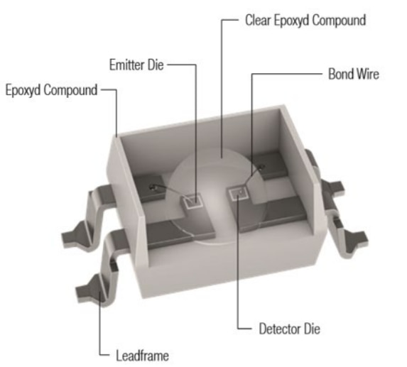
Figure 1: WL-OCPT Optocoupler Construction
The device’s principle of operation is simple: an electrical-tooptical conversion takes place in the emitter, as the IR-LED emits infrared radiation (i.e. photons) with an intensity proportional to the current flowing through it. These photons travel through the optical medium, and after reflection on the dome’s inner surface, they reach the photosensitive basecollector area of the phototransistor. Here, an optical-toelectrical conversion takes place, as the phototransistor’s valence electrons ‘absorb’ the photons’ energy and ‘jump up’ to the conduction band, generating a current across collector and emitter in a process similar to that of a standard ‘npn’ bipolar junction transistor (BJT). The ratio between the phototransistor collector current (IC) and the IR-LED current (IF) represents the main optocoupler parameter: the currenttransfer-ratio (CTR). The electrical symbol of a phototransistor optocoupler is shown in Figure 2.
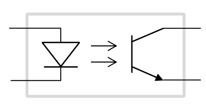
Figure 2: Electrical symbol of a Phototransistor Optocoupler
03. THE CURRENT-TRANSFER-RATIO (CTR)
3.1 What is CTR?
The CTR is the current gain parameter of the optocoupler, expressed as the ratio of collector current (IC) to LED current (IF):
 (1)
(1)
It must be noted that Equation (1) is valid when the phototransistor is biased within its active region of operation (see section 07). By analogy, the CTR is equivalent to the static ‘Hfe’ or ‘ß’ (beta) parameter of a bipolar junction transistor, while the LED current would be equivalent to the BJT base current. Therefore, from a functional point of view the optocoupler can be considered like an ‘isolated-base’, npn-type BJT. Note also that the CTR is commonly expressed as a percentage (%), as follows:
 (2)
(2)
One of the main challenges when designing with optocouplers is the wide tolerance and variations of its CTR value, caused by several factors as explained next.
3.2 CTR Production Tolerance and Device Binning
Inherent limitations in semiconductor manufacturing processes make it difficult to produce devices with identical characteristics and parameter values. IR-LEDs are grown on GaAs-substrate wafers, in which obtaining a completely uniform semiconductor doping and layer thickness becomes a challenge. This results in different current-to-light conversion efficiencies for each LED device on the wafer (i.e. different photonic energy emitted by each LED for a set current level). Similar limitations apply regarding the phototransistor, resulting in devices with different light sensitivity (i.e. generating a different collector current for the same oncoming photonic energy). These two factors directly impact the CTR tolerance out of production, but they are not the only ones, as for example variations in the transmittance and reflectivity parameters of the clear epoxy compound dome optically linking the LED and phototransistor also contribute to increase the CTR production tolerance of the device.
Since an overly wide tolerance is not practical in most designs, the CTR of each optocoupler is measured in production at a set DC operating point and the device is classified within a binning based on the measured value. Each binning guarantees a maximum and minimum CTR under the test conditions indicated, and it is specified with a suffix letter, as shown in Table 1 for the WL-OCPT 816 series. Although this reduces the initial tolerance range to consider in a design, the CTR also depends on operating conditions like DC-bias and temperature, and these variations also need to be considered.
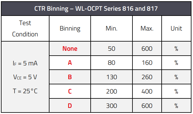
Table 1: Example of Optocoupler CTR binning (WL-OCPT 816/817 series)
3.3 CTR variation with LED current
The CTR range within a binning is only valid for a set LED current (IF) and collector-emitter voltage (VCE). For the WL-OCPT series, this is 5 mA and 5 V, respectively. For a different LED current, the CTR range obtained would be different, as it can be observed in Figure 3, where the absolute CTR as a function of LED current of one sample from each binning is shown, obtained at a constant VCE = 5 V. It can be seen how the CTR increases with LED current until a certain point above which the behavior is inverted, and a further increase in LED current causes a decrease in the CTR. This is due to the non-linear current-to-light conversion efficiency of the LED combined with the variation of the phototransistor gain. It is observed how for IF = 5 mA, the CTR of each device is found within the range of the corresponding binning, as expected.
As the phototransistor enters the saturation region of operation, the CTR value and characteristic curve also changes, as shown in Figure 4 for VCE = 0.4 V. The CTR is lower and the curve peaks at a lower LED current.
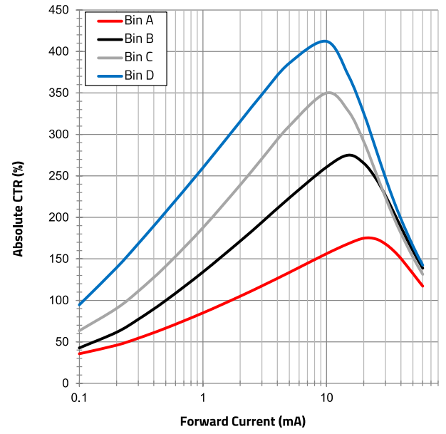
Figure 3: Absolute CTR vs. IF (@VCE= 5 V, T=25°C) (WL-OCPT 817)
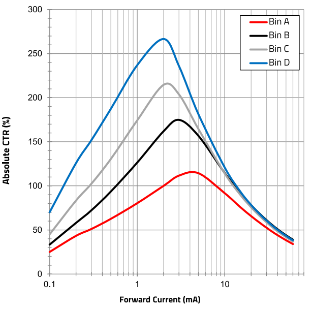
Figure 4: Absolute CTR vs. IF (@VCE= 0.4 V, T=25°C) (WL-OCPT 817)
Note that the curves of Figure 3 and Figure 4 correspond to only one sample device from each binning. Curves for relative CTR are also provided in the WL-OCPT series datasheet, in which the CTR is normalized to the value measured at IF = 5 mA. Figure 5 shows that for an LED current below 10 mA and with the phototransistor operating in the active region (VCE=5 V), all normalized curves are very close together independent of the binning. Knowing that the relative CTR curve of a binning does not practically change with absolute CTR value in this range, it can then be used to estimate the absolute CTR of any device withing the binning, as follows:

Note that above 10 mA, the relative curves show a stronger variation with absolute CTR value, and so E.3 will be less accurate in that range. When the phototransistor operates in saturation (Figure 6), the curve characteristic is somehow inverted, and E.3 is only accurate above approximately 5 mA.
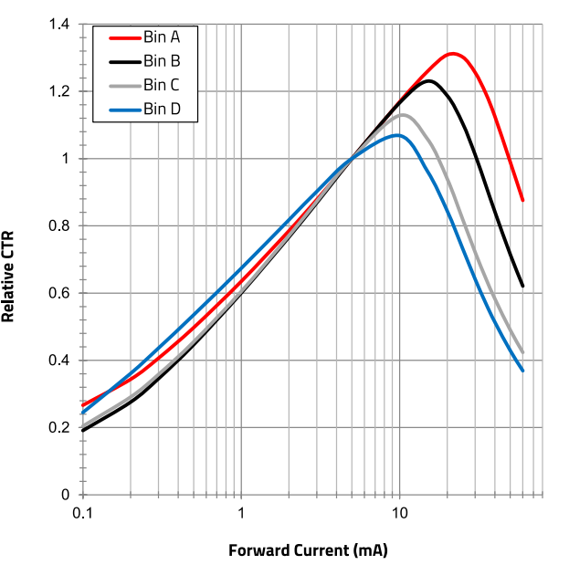
Figure 5: Relative CTR vs. IF (@VCE = 5 V, T=25°C) (WL-OCPT 817)
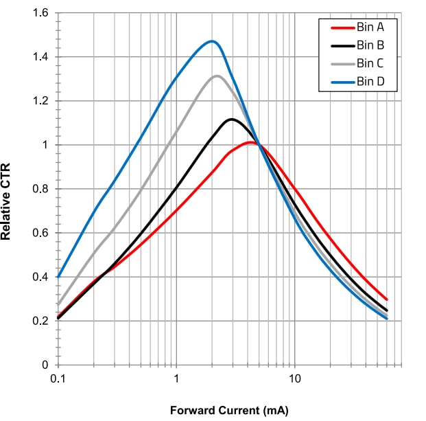
Figure 6: Relative CTR vs. IF (@VCE= 0.4 V, T=25°C) (WL-OCPT 817)
3.4 CTR variation with Temperature
The operating temperature of the device affects both, the LED emission efficiency as well as the phototransistor light-to-current gain, impacting with it the optocoupler CTR in a non-linear manner, as shown in the relative CTR curves of Figure 7. Both curves are valid for all binnings and for an LED current below approximately 5 mA. Note that here the operating ambient temperature is considered, with the device junction temperature directly proportional to it.
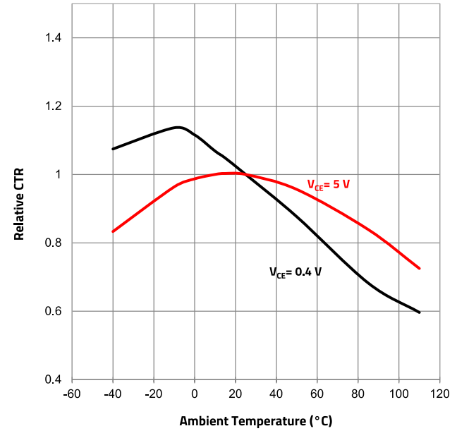
Figure 7: CTR vs Temp (@ IF =5 mA)
3.5 Measuring CTR
Measuring the CTR for the specific DC-Bias condition of the application is straight-forward when measuring the currents based on Equation (1), as it is also for the recommended setup shown in Figure 8 using only voltage probes. Here, a common-collector configuration is used. The output resistor R2 as well as the bias voltage Vdd are both set as in the end application circuit where the optocoupler is used, and the LED resistor R1 is selected of the same value than R2. The DC input voltage supply (Vs) is then increased until the collectoremitter voltage (VCE) reaches the target value. The CTR at this DC-bias condition is then obtained as:
 (4)
(4)
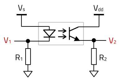
Figure 8: Recommended setup for CTR measurement
3.6 Example: CTR Range Estimation
In order to ensure circuit functionality, the worst-case CTR range must be estimated considering all operating conditions of the design.
A conservative, good approach for this is to use optocoupler samples with a CTR slightly above and below the limits of the selected binning. For example, if the binning selected is the Bin B (1.3 (130%) < CTR < 2.6 (260%)), then a sample from Bin A with CTR around 1.3 or slightly lower, and a sample of Bin C with CTR around 2.6 or slightly higher can be used. With the two samples above, the maximum and minimum CTR at the specific operating conditions of the design can be directly measured. Note that for some CTR values there is a small overlap between binnings, as shown in previous Table 1. For example, a device with a CTR of 2.2 could be classified within Bin B or C, indistinctly.
Alternatively to the approach above, if the collector-emitter voltage is around 5 V, the relative CTR curves provided on the WL-OCPT datasheet can be directly used. As an example, consider the device WL-OCPT 140816141310 (Bin C) and the following design specification:
- IF = 2 mA
- VCE = 5 V
- T = -20 to +80°C
For the Bin C with IF = 5 mA and based on Table 1, the CTR range is 200 to 400% (i.e. 2 to 4). The normalized curve indicates that for IF = 2 mA, the CTR should be multiplied by a factor of KCTR_2mA = 0.76 (Figure 9). Similarly, the temperature curve normalized to T = 25°C shows a worst-case minimum scaling factor of Kt_min = 0.85 and maximum of Kt_max = 1 for the temperature range considered (Figure 10).
The following expressions are used to calculate the CTR limits:
 (5)
(5)
 (6)
(6)
Substituting values, it is obtained:

Note that this procedure can also be used for different collector-emitter voltages as long as the phototransistor is biased within the active region and the LED current is lower than 10 mA, since under those conditions the CTR will vary only slightly with changes in VCE.
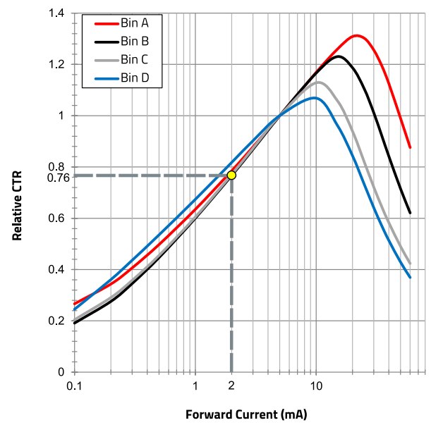
Figure 9: Relative CTR Factor for IF = 2 mA (@ T=25°C)
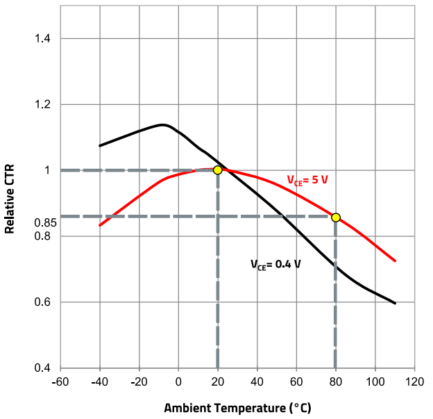
Figure 10: Maximum and Minimum relative CTR for the range -20°C to +80°C (IF=5mA)
3.7 The AC or small-signal CTR
Up to this point, only the DC or static CTR was considered. Note that if after DC-biasing the optocoupler as in Figure 8, a low-frequency (e.g. 100 Hz), small-amplitude sinusoidal current is superimposed to the DC LED current, it will also be transferred to the output with a specific gain or attenuation. If both resistors R1 and R2 are again selected of the same value for the measurement, the small-signal CTR of the device at this DC operating point is obtained as in Equation (7), where ΔV1 and ΔV2 are the peak-to-peak amplitudes of the sinusoidal voltages across R1 and R2, respectively:
 (7)
(7)
Figure 11 shows measurement results for a WL-OCPT 817 Bin A sample device, DC-biased at IF = 3 mA and VCE = 5 V with RF= RC = 1 kΩ. Note that with these values and based on previous Figure 8, in Figure 11 the measured ‘V’ units represent ‘mA’, and ‘mV’ represent ‘µA’. It is observed how IC = 2.89 mA, resulting in a DC CTR of 0.96, whereas the small-signal CTR is higher at around 1.23 (230 µA/187 µA).
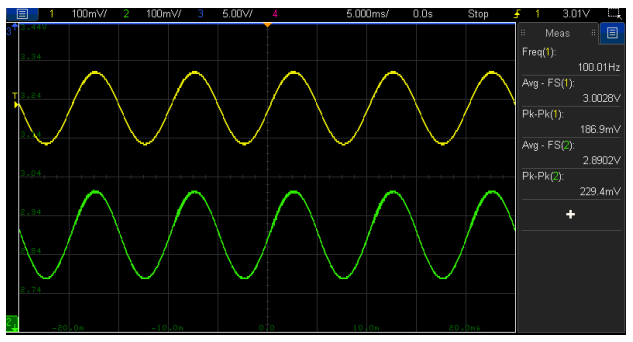
Figure 11: Results at VCE = 5 V for WL-OCPT 817 Bin A (VR1 (yellow), VR2 (green))
The difference observed between the DC and AC CTR values is mainly due to the rapid collapse of the CTR at very small LED currents. Figure 12 shows the collector current as a function of the LED current for VCE = 5 V. Here, every point of the curve gives the DC-CTR as the ratio IC/IF at that point, whereas the AC-CTR corresponds to the slope of the curve at that point (i.e. dIC/dIF). Note that if the plot were exactly linear with a constant slope right from the start at very low LED currents, then the small-signal and the DC-CTR at any point would be the same. For further insight, Figure 13 shows the DC- and AC-CTR plotted as a function of LED current for the same device. Note that although in this plot, above 1.5 mA the AC and DC-CTR appear related with a constant of proportionality, this is not always the case and the relationship over the full current range may vary, for example, as the DC operating point approaches the saturation region. This can be observed in Figure 14, with results from a Bin D device biased at VCE = 2.5 V.
When the optocoupler is used to transmit a signal which has both DC and AC components, like in the case of Figure 11 or in some switching applications for example, then the two CTR values should be used accordingly for the calculations.
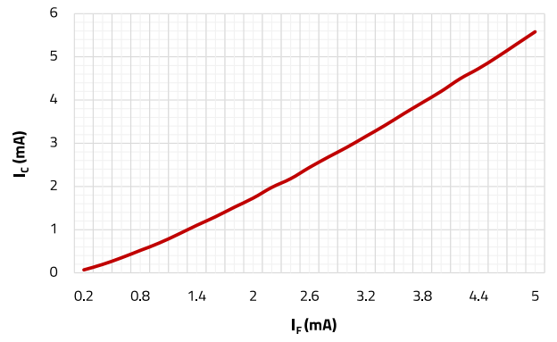
Figure 12: IC vs IF at VCE = 5 V for WL-OCPT 817 Bin A
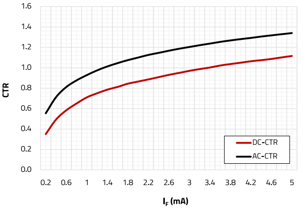
Figure 13: AC- and DC-CTR at VCE = 5 V for WL-OCPT 817 Bin A
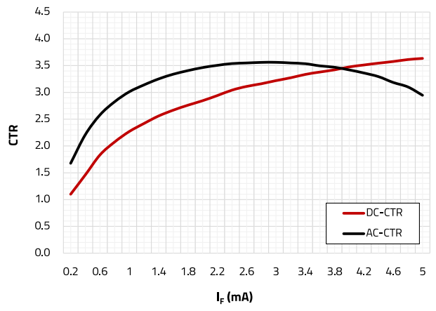
Figure 14: AC- and DC-CTR at VCE = 2.5 V for WL-OCPT 817 Bin D
04. FREQUENCY RESPONSE AND BANDWIDTH
4.1 Parasitic capacitance and cutoff frequency
In the previous section, the small-signal CTR was measured at a low frequency. However, if the frequency is steadily increased, a point will be reached above which the sinusoidal signal will become attenuated and phase-shifted at the output (phototransistor side).
The reason for this is the total parasitic capacitance across collector and emitter terminals of the phototransistor (Copto), affected mainly by the base-collector capacitance of the device. This capacitance, together with the output bias resistor RC, forms a low-pass filter which limits the optocoupler bandwidth. This is also referred as a ‘pole’ in control systems, and it is an important design factor in applications like isolated communication interfaces as well as feedback loop compensation of isolated power supplies. Irrespective of whether the optocoupler is biased in a common-emitter or a common-collector circuit configuration, the equivalent small-signal AC circuit is the same as shown in Figure 15.

Figure 15: Optocoupler Equivalent Small-Signal AC Circuit
In this optocoupler AC model, the IR-LED is replaced by its dynamic resistance rd, which is typically much lower than RF for high-enough LED currents (well above the knee of its I-V curve). The phototransistor is modelled as a dependent current-source with a value set by the optocoupler AC-CTR and LED current. For AC analysis, Copto is in parallel with RC. The input-to-output transfer function is obtained by analyzing this circuit in the s-domain (Laplace transform analysis). Simplifying for RF >> rd, it is obtained:
 (8)
(8)
This has the structure of a typical first-order or single-pole system as shown in Equation (8), with a low-frequency gain G0 which depends on the optocoupler small-signal CTR and the input and output bias resistors, and a cutoff frequency fopto set by Copto and RC. Observe that if RF = RC, then G0 directly corresponds to the AC-CTR of the device.
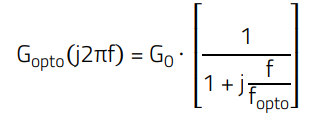 (9)
(9)
 (10)
(10)
 (11)
(11)
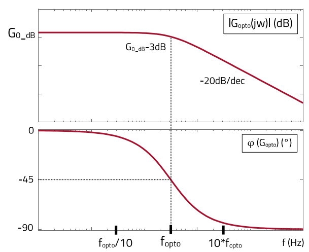
Figure 16: Optocoupler Input-Output Frequency Response
The Bode plot of the magnitude and phase versus frequency of Equation (9) is shown in Figure 16. Note how the phase starts changing one decade before fopto, at which the amplitude has already been attenuated to 70% (-3 dB) of its initial low-frequency value.
Figure 17 shows how the optocoupler cutoff frequency theoretically decreases as the load resistor value increases. A lower RC will result in higher fopto and bandwidth, albeit at the cost of higher collector current resulting in higher power dissipation.
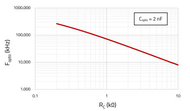
Figure 17: Optocoupler Pole Frequency vs Load Resistor (RC)
4.2 Measuring optocoupler frequency response
An accurate method for characterizing the optocoupler frequency response uses a vector network analyzer (VNA) together with a DC-bias injector or an injection transformer as shown in Figure 18. The AC-sweep signal, injected via the transformer, appears as an AC voltage across the resistor Rin, which is typically selected between 10 Ω and 100 Ω. The resulting AC voltages across RF and RC are then measured. The devices used for the measurements shown in this document were the Bode100 and B-WIT-100
injection transformer, both from Omicron Lab.
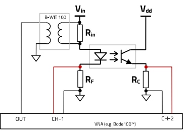
Figure 18: Optocoupler Frequency response Measurement setup (VNA)
Note that before performing the measurement, the optocoupler must be DC-biased as in the target application circuit, and it needs to be ensured that the sinusoidal voltage waveforms observed across RF and RC at a frequency much lower than the cutoff frequency (e.g. 100 Hz) are not distorted. If that is the case, then Rin and/or the amplitude of the injected signal would need to be reduced. This issue is particularly common when the phototransistor is DC-biased close to the saturation or cutoff regions of operation. As a rule-of-thumb, the injected sinusoidal amplitude should be set as low as practically possible (small-signal), while still high enough to prevent noise from corrupting the measurement result.
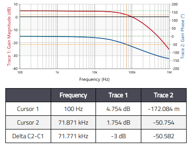
Figure 19: Example Measurement Results with VNA (Bode100)
In Figure 19, experimental results for a WL-OCPT device from Bin B (140817140210) are shown, with RF = RC = 1 kΩ and DC-bias conditions of IF = 1 mA, IC = 1.25 mA and VCE = 5 V. A cutoff frequency of 71.8 kHz is observed. Note how the high-frequency portion does not exactly match the analytical graph of Figure 16. This is because the optocoupler has another pole at higher frequency causing a steeper gain rolloff and additional phase lag, but was not included in the analytical model.
Figure 20, Figure 21 and Figure 22 show the sinusoidal voltage waveforms across RF and RC for the previous measurement at three different frequencies. In Figure 20, at 100 Hz, both waveforms are in phase and it is observed a reference ΔVRC around 260 mV. Figure 21 shows the waveforms at fopto = 72 kHz, where ΔVRC has decreased as expected by around 30% to 182 mV and its phase has shifted approximately 50° from the low-frequency reference (2 µs of a 14 µs period). If the test frequency is further increased to 120 kHz as shown in Figure 22, then ΔVRC is further reduced and the phase shift increases in this case to around 70° (1.62 µs of 8.33 µs).
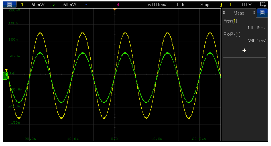
Figure 20: Reference amplitude at f = 100 Hz (VRF (green) , VRC (yellow))
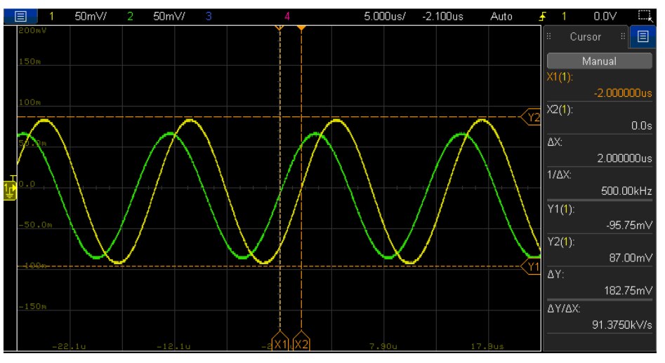
Figure 21: Waveforms at fopto ≈ 72 kHz (VRF (green) , VRC (yellow))
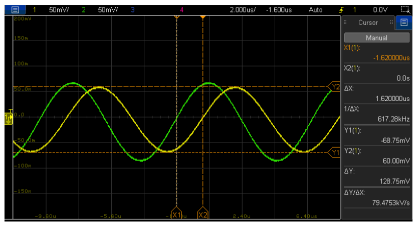
Figure 22: Waveforms at f = 120 kHz (VRF (green) , VRC (yellow))
4.3 Cutoff frequency variations
The optocoupler parasitic capacitance Copto and in turn fopto vary with the CTR of the device (binning) as well as its DC-bias and operating temperature. Figure 23 shows, for a set DC-bias condition, how a device from a higher CTR binning results in a higher fopto, while the difference amongst the binnings becomes smaller as the current reduces. For a specific device, the bandwidth increases with IC up to a point above which a plateau in the curve is reached and it stabilizes. Conditions for these measurements were VCE = 5 V and RC = 1 kΩ.
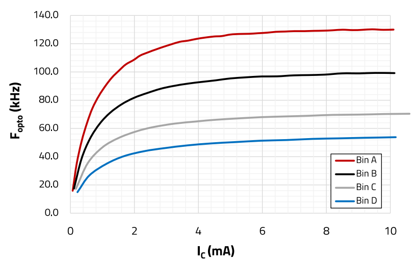
Figure 23: Fopto vs IC (@VCE = 5 V, RC = 1 kΩ)
Figure 24 shows, for the Bin A sample device, how fopto increases with VCE especially at higher LED and collector bias currents, while it remains practically unaffected at low currents. In Figure 25, for the same Bin A device biased at VCE = 5 V and IF = 2 mA (at 25°C), it can be seen how fopto reduces from 106 to 72 kHz as its operating temperature increases from 25 to 85°C. All such variations should be carefully considered in the design to ensure correct operation for all expected operating conditions. Based on these results, if a high bandwidth is required, then a device from a lower CTR binning should be the preferred choice, while ensuring high-enough phototransistor current and operation at a lower temperature. If a smaller variation of the cutoff frequency is more important, then operation at low collector current (and in turn, low LED current) seems to be of advantage.
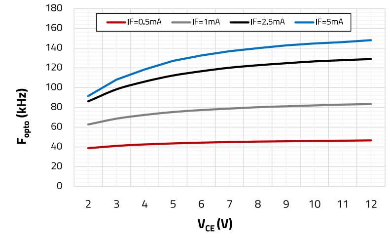
Figure 24: Fopto vs. VCE (WL-OCPT 817 Bin A, RC = 1 kΩ
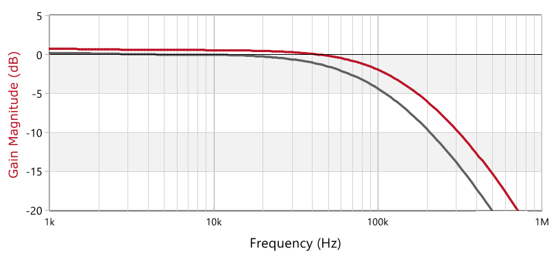
Figure 25: Bin A - Fopto at T = 25°C (106 kHz) and T = 85°C (72 kHz) (RC = 1 kΩ)
05. SWITCHING TIME
In some applications like motor control, relays and communication interfaces, the optocoupler is used as an isolated electronic switch, where the phototransistor is driven into conduction and blocking states based on the LED control signal. However, the phototransistor cannot follow the changes in LED current instantaneously, as there is a time delay until its collector-emitter voltage starts to change, and it does it at a specific slew-rate as its parasitic capacitance charges or discharges. Figure 26 shows a typical switching test circuit in a common-emitter configuration, where the optocoupler LED is driven with a square waveform (Vin) whose amplitude (ΔVin) is adjusted based on the target operating point, and the voltage across RF is measured as an image of the LED current. The typical switching diagram is shown in Figure 27. The rise and fall times of the output voltage (Vout) are expressed with the parameters tr and tf respectively, with the rise time corresponding to the time it takes for the output voltage to rise from 10 to 90% of its final value, and conversely, to fall from 90 to 10% of Vout for the fall time. The total on and off times (ton and toff) correspond to the time elapsed from the moment the LED current starts to change until when Vout reaches 90% (turn-on) or 10% (turn-off) of its final value, respectively.
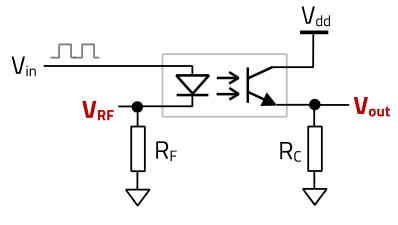
Figure 26: Optocoupler Switching test setup
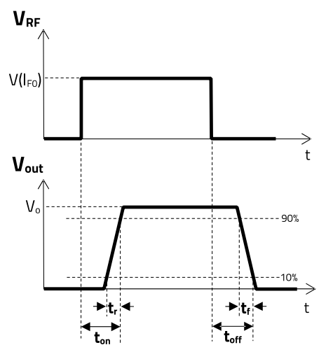
Figure 27: Optocoupler Switching Reference Diagram
Figure 28 and Figure 29 show example experimental results for the turn on and off transitions, respectively, for the sample device WL-OCPT 817 from Bin B and with ΔVin = 5 V (50% duty-cycle), Vdd = 7 V, RF = RC = 1 kΩ and VCE_on = 0.6 V. Note that VCE_on refers to the collector-emitter voltage when the phototransistor is in conduction state. A turn-on time of 5 µs, with a rise time of 3.6 µs is measured, whereas the off-time is 5.7 µs with a fall-time of 3.8 µs. It can be seen in both cases how the switching time of the device is primarily affected by the phototransistor response and not by the LED.
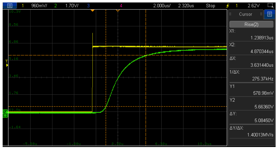
Figure 28: Turn-on example (WL-OCPT 817 Bin B) (VRF (green) , VRC (yellow))
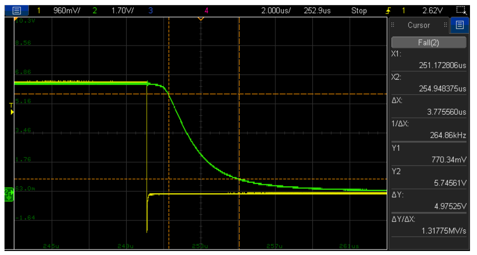
Figure 29: Turn-off example (WL-OCPT 817 Bin B) (VRF (green) , VRC (yellow))
5.1 Switching time variations
The switching time is closely related to the optocoupler bandwidth (fopto), and as a result, it is also affected by the same parameters. Figure 30 shows the dependence of the turn on and off times with the load resistance for a WL-OCPT 817 Bin B device at T = 25°C. The phototransistor DC-bias is kept constant at IC = 2 mA and VCE_on = 2 V by adjusting ΔVin and Vdd as necessary while RC is varied. It is observed how a lower value of RC results in a faster swiching speed.
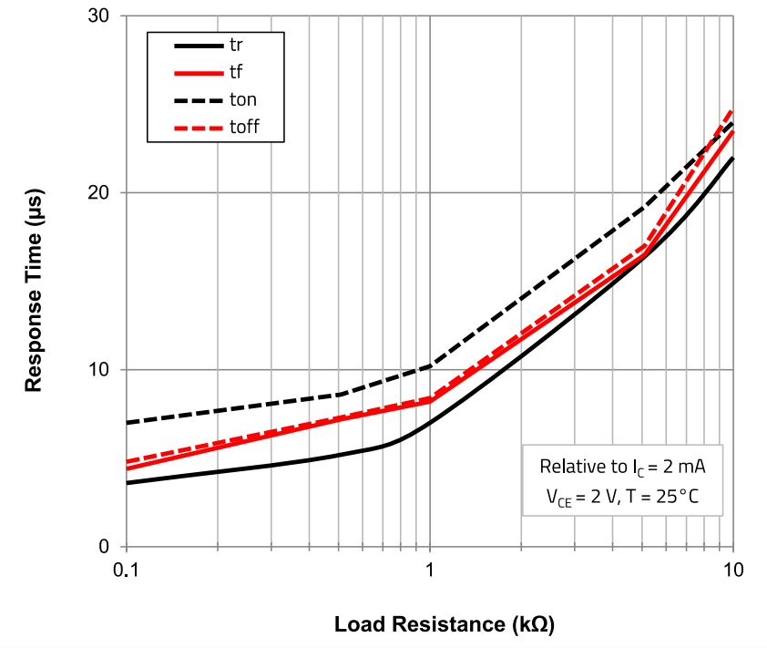
Figure 30: ton, toff tr and tf vs RC (WL-OCPT 817 curve)
The CTR also affects fopto and in turn the switching speed. This can be observed in Figure 31 and Figure 32, which show the turn-off transition of two devices from Bin A and Bin D, respectively. Test conditions are ΔVin = 5 V, Vdd = 3.3 V and RF = RC = 1 kΩ. Both devices are driven into saturation when switching, with VCE_on = 0.3 V for Bin A device and VCE_on = 0.2 V for Bin D device, and it can be seen how a faster fall-time and total turn-off switching speed is achieved with the Bin A device, with toff being around 12 µs versus 4.6 µs, in this case.
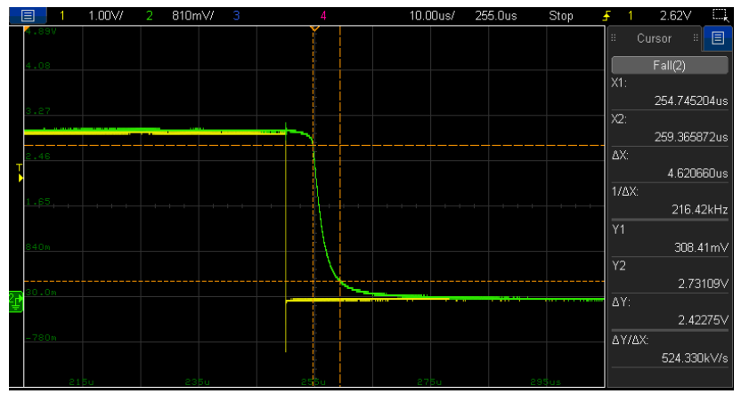
Figure 31: Turn-off transition (Bin A, VCE_on = 0.3 V) (VRF (green) , VRC (yellow))
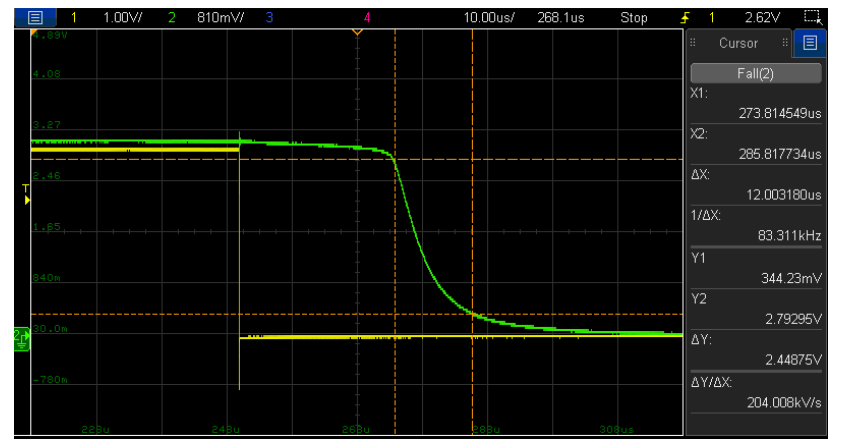
Figure 32: Turn-off transition (Bin D, VCE_on = 0.2 V) (VRF (green) , VRC (yellow))
Special attention requires the much longer delay time (td_off= toff - tf) observed for the Bin D device. If VCE_on is increased to 1 V, the delay time dramatically shortens, as shown in Figure 33. In the results of previous Figure 30, td_off was negligible (i.e. toff ≈ tf) because in the test the phototransistor was being driven with a higher VCE_on = 2 V. However, the deeper into saturation the phototransistor is driven (i.e. the lower VCE_on), the longer the delay and total switching time. This behavior is shown in Figure 34 for the same Bin D device, tested with a fixed ΔVin = 5 V and RF = RC = 1 kΩ. It is observed how td_off and in turn toff dramatically increase as VCE_on decreases, especially below 0.8 V. Above 1 V, the delay time is negligible and the turn-off time is mostly dominated by the fall-time. Note that this characteristic will vary for another device from a different CTR binning and operating conditions, so it needs to be studied for each particular case. However, as a general rule-of-thumb, if a high switching speed is paramount to the application then it is advised to use a device from a lower CTR binning as well as not to unnecessarily drive the phototransistor too deep into saturation.

Figure 33: Turn-off transition (Bin D, VCE_on = 1 V) (VRF (green) , VRC (yellow))
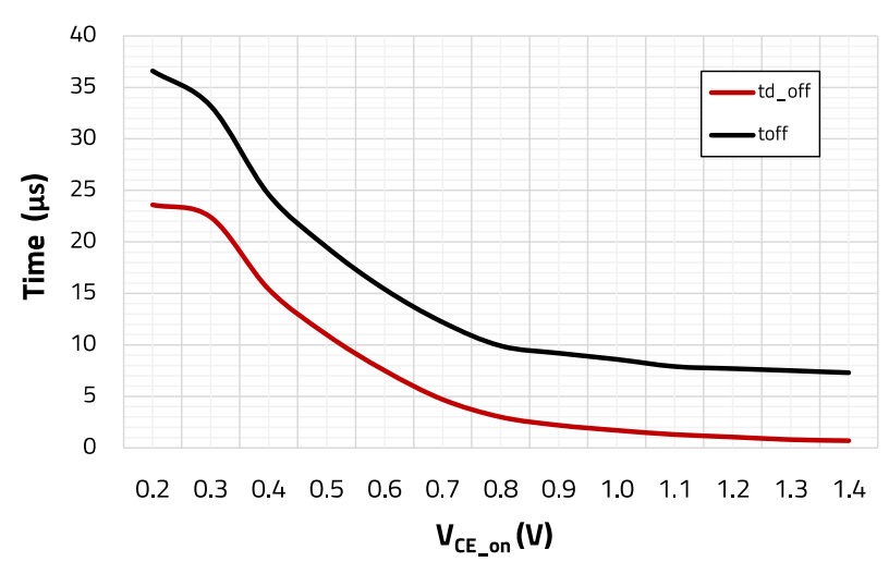
Figure 34: td_off and toff times vs. VCE_on (Bin D)
06. ADDITIONAL PARAMETERS
Some electrical ratings and parasitic element specifications found in the WL-OCPT datasheet are explained in more detail here:
- Input peak forward current (IF_peak): the maximum LED peak current rating based on a pulsed current of 10% duty cycle at the specified frequency. Important for switching applications.
- Input reverse voltage: maximum reverse voltage that the IR-LED can withstand. Since it is only 6 V, careful design is required in switching applications in order to prevent reverse voltage spikes exceeding this value. Adding an antiparallel diode is a typical protection solution (Figure 35).
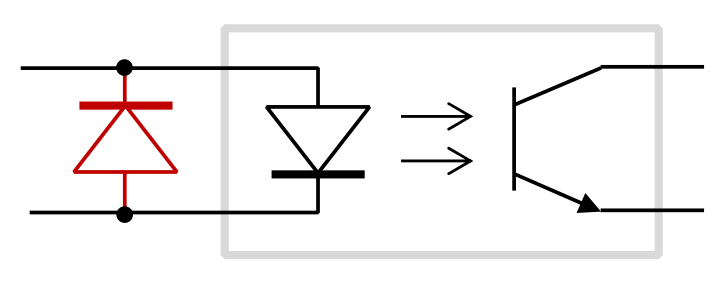
Figure 35: Antiparallel protection diode
- Collector-emitter dark current (ICEO-Dark): the leakage current flowing through the phototransistor with zero IR-LED current. It increases with the applied collectoremitter voltage and ambient temperature, as shown in the curve provided in the WL-OCPT datasheet.
- Input capacitance (Cin): the parasitic junction capacitance of the IR-LED. Its value depends on the forward and reverse voltage applied to the device. For the WL-OCPT datasheet value, the test conditions are Vf = 0 V, T = 25°C and f = 1 kHz.
- Floating Capacitance (CIO): the parasitic capacitance across the isolation barrier of the optocoupler, this is, between the IR-LED and the phototransistor. The lower the value of CIO, the higher the common-mode noise rejection (CMRR) of the device. A low CIO is important in applications where very high dv/dt transients across input and output of the optocoupler are generated, like for example, highside isolated gate driver systems in power inverters with very fast switching speeds. In such cases, a high common-mode-transient-immunity (CMTI) is typically required. In addition, high CIO also has an impact on EMI and common-mode noise.
- Isolation voltage (VISO): This is the maximum voltage which can be safely applied across input and output of the optocoupler based on compliance with the partial discharge test specified on the EN 60747-5-5 standard.
- Isolation Resistance (RISO): it is a measure of the electrical resistance of the epoxy compound dome covering the IR-LED and phototransistor. Its value is obtained by applying 500 VDC across the IR-LED and phototransistor terminals and measuring the resulting DC leakage current.
07. OPTOCOUPLER DC-BIAS
7.1 DC-Bias Circuit and Operating point
Biasing an optocoupler is equivalent to biasing a BJT transistor, but considering the IR LED current as the equivalent BJT base current. Common-emitter (CE) and common-collector (CC) are the typical configurations to DC-bias the optocoupler, as shown in Figure 36 left and right, respectively. The connection of the output resistor RC is done to the collector or to the emitter nodes of the phototransistor, changing with it the output voltage node. Based on this, as the LED current rises, the output voltage would decrease in a common-emitter circuit, while it would increase in a common-collector configuration. Considering a low-frequency sinusoidal input signal (i.e. more than a decade lower than the optocoupler pole frequency), the output signal would be inverted (i.e. -180° phase shift) in a common-emitter circuit.
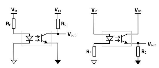
Figure 36: Optocoupler bias circuit: common-emitter (CE) (left), common-collector (CC) (right)
The phototransistor can operate at any given instant in one of the three regions of its IC/VCE curve, as shown in the approximation of Figure 37. They are differentiated depending on the values of collector-emitter voltage (VCE) and collector current (IC), as follows:
- Saturation Region: VCE ≤ VCEsat & IC < CTR∙IF
- Cut-off Region: VCE > 0 & IF = 0, IC ≈ 0
- (Forward) Active Region: VCE > VCEsat & IC ≈ CTR∙IF
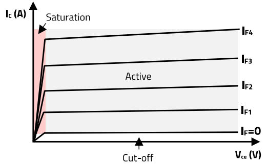
Figure 37: Phototransistor Operating Regions (IC/VCE Curve at IF)
For a fixed Vdd and RC, the DC operating point and thus, the region of operation will be set by the LED current IF. In the active region for example, an increase of IF causes lower VCE and higher IC, whereas reducing IF results in higher VCE and lower IC, as shown in Figure 38. Note also how the DC-bias slope can be further adjusted with Vdd and RC. The device will have to be DC-biased in order to operate in the target region(s) required by the specific application.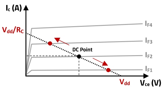
Figure 38: Optocoupler DC-bias point
7.2 DC-Bias for Switching/Logic Operation
When using the optocoupler in a switching application, the operating point would normally alternate between the cutoff and saturation regions, depending on whether the device output must be set high or low. Whatever configuration is used, it is important to analyze the worst-case output voltage level when the phototransistor is in its conduction state. In a CE configuration this corresponds to an output ‘low’, whereas for CC to an output ‘high’, with the following values for CE (Equation (12)) and CC (Equation (13)), respectively
 (12)
(12)
 (13)
(13)
In both cases, RF sets the target LED current as:
 (14)
(14)
The LED current is linked to the LED foward voltage (VF) and temperature as shown in Figure 39. Note that a lower LED current means lower power loss and longer optocoupler useful life, but typically at the expense of a lower bandwidth. Note how in both cases, the output voltage also depends on the CTR. Especially for CE configuration, it is important to estimate both the maximum CTR and the minimum IF values to ensure that at the worst-case scenario, the output ‘lowstate’ voltage will still be lower than the maximum value accepted by the respective load as a ‘low-state’. This could be for example the minimum gate threshold voltage of the MOSFET in a motor control application or the maximum ‘zero’ limit of the MCU port in an interface application. The minimum value for the output resistor RC in a CE circuit can then be calculated:
 (15)
(15)
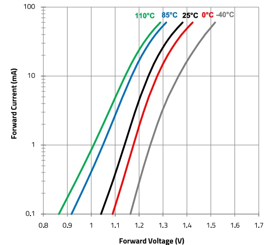
Figure 39: IF vs. VF (at Temperature)
Regarding the CC configuration, the limitation corresponds to the output ‘high’ scenario. In order to ensure that the minimum output voltage (Vout_on_min) for an output ‘high’ state lies above the minimum acceptable for the design, the maximum CTR and minimum IF values need to be estimated. The minimum value for the output resistor RC in a CC circuit is then calculated:
 (16)
(16)
As seen in previous Figure 30, care should be taken not to select a too high RC value, as it will slow down the switching speed. Also observe how, the lower CTRmax is, the lower RC needs to be set. This shows that devices from a lower CTR binning should be the preferred choice where possible, since these not only have the advantage of a lower Copto and thus higher switching speed, but they can be used with a lower RC, allowing for an even faster switching transition.
7.3 DC-Bias for Analog/Linear Operation
In order to transfer an analog signal, be this DC or AC, the phototransistor is biased within its active region of operation. This is also called the linear region, as it is characterized by an almost linear relationship between IF and IC (offset aside). In Figure 40, test results are shown for a WL-OCPT 817 Bin A device, where the LED current is ramped up from 3.4 mA to 8.3 mA, and it is observed how the phototransistor current follows it very closely (superimposed to IF for better insight). Here both currents are measured as voltages across RF and RC, both 1 kΩ, in a common-collector configuration. Note that Vdd is fixed but VCE changes depending on the current, as per previous Figure 38. With ΔIC ≈ 7.25 mA and ΔIF ≈ 4.85 mA, an average CTR of around 1.5 is observed in this current range.
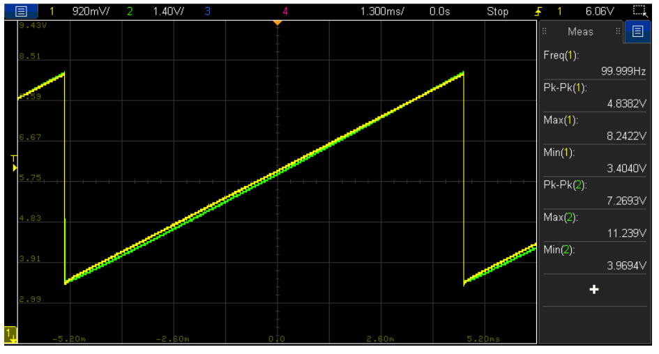
Figure 40: IF and IC in active region (VRF (green) , VRC (yellow))
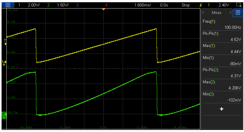
Figure 41: IF and IC in active region extending into cutoff and saturation at the extremes (VRF (green) , VRC (yellow))
When operating at very low currents, linearity will degrade, as it will also be the case when fully extending the range of operation close or into the cutoff and saturation regions, as observed in Figure 41. Note also that these measurements correspond to a single optocoupler device at 25°C operating temperature. However, the CTR varies non-linearly with temperature, not forgetting the effect of the CTR tolerance within a binning which also needs to be considered in a design.
08. WL-OCPT SPICE MODELS
SPICE models are provided for each series of the WL-OCPT, both for LTspice as well as PSPICE
simulators. Within a series, a different SPICE model is provided for each binning. In LTspice
for example, after selecting the series, the binning can then be selected from the ‘Component Attribute Editor window’, from the drop-down list which opens after double left-click on the ‘SpiceModel’ value field, as shown in Figure 42.
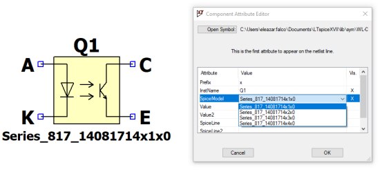
Figure 42: Selecting the WL-OCPT 817 device binning in LTspice
Each model corresponds to a sample device with a nominal CTR within the expected range of the binning at VCE = 5 V, IF = 5 mA. For the 817 and 816 models, nominal CTR values modelled are approximately 1.4 for Bin A, 2.3 for Bin B, 3.2 for Bin C and 4 for Bin D.
Figure 43 shows the absolute CTR vs. LED current curves obtained in an LTspice simulation for each 817 device binning at VCE= 5 V. Figure 44 shows the simulated frequency response for a Bin B device biased at IC = 2 mA and VCE = 5 V, as a function of RC (100 Ω, 1 kΩ, 10 kΩ and 30 kΩ). The curves are in good agreement with those from the reference measurement samples shown in the datasheet. Although SPICE models help in the design process, it is important to understand that they only represent an approximation of the behavior of the device, and some parameter dependencies (e.g. temperature) may not be modelled. For this reason, final validation must always be performed experimentally with physical samples.
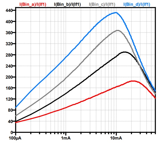
Figure 43: CTR vs. LED current curves (LTspice )
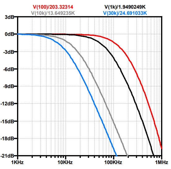
Figure 44: Normalized frequency response for Bin B and Rc = 100 Ω (l), 1 kΩ (l), 10 kΩ (l) and 30 kΩ (l) (LTspice)
09. THE WL-OCPT SERIES
The WL-OCPT (Opto-Coupler Photo-Transistor) is a series of optocouplers with phototransistor-output configuration. In addition to the unipolar input current variant, two series are offered accepting bidirectional input current, as shown in Figure 45. The device series are offered in various package types and with different ratings mainly regarding CTR range, Vce as well as primary-to-secondary isolation voltage (Viso), and an overview of these is provided on the table in Table 2. These are general-purpose devices targeting many different isolated applications like low-speed communication interfaces, sensor systems, motor drives and relays, industrial PLCs I/O modules, Power-over-Ethernet, AC-Mains monitoring and power supplies, amongst others. For further information about WL-OCPT series and for ordering free samples, please visit the WL-OCPT section on Würth Elektronik website here.

Figure 45: WL-OCPT Unipolar Input (left) and Bipolar Input (right)
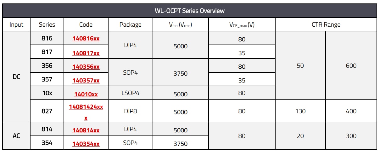
Table 2: WL-OCPT series overview (Status on May-2023)
IMPORTANT NOTICE
The Application Note is based on our knowledge and experience of typical requirements concerning these areas. It serves as general guidance and should not be construed as a commitment for the suitability for customer applications by Würth Elektronik eiSos GmbH & Co. KG. The information in the Application Note is subject to change without notice. This document and parts thereof must not be reproduced or copied without written permission, and contents thereof must not be imparted to a third party nor be used for any unauthorized purpose. Würth Elektronik eiSos GmbH & Co. KG and its subsidiaries and affiliates (WE) are not liable for application assistance of any kind. Customers may use WE’s assistance and product recommendations for their applications and design. The responsibility for the applicability and use of WE Products in a particular customer design is always solely within the authority of the customer. Due to this fact it is up to the customer to evaluate and investigate, where appropriate, and decide whether the device with the specific product characteristics described in the product specification is valid and suitable for the respective customer application or not. The technical specifications are stated in the current data sheet of the products. Therefore the customers shall use the data sheets and are cautioned to verify that data sheets are current. The current data sheets can be downloaded at www.we-online.com. Customers shall strictly observe any product-specific notes, cautions and warnings. WE reserves the right to make corrections, modifications, enhancements, improvements, and other changes to its products and services. WE DOES NOT WARRANT OR REPRESENT THAT ANY LICENSE, EITHER EXPRESS OR IMPLIED, IS GRANTED UNDER ANY PATENT RIGHT, COPYRIGHT, MASK WORK RIGHT, OR OTHER INTELLECTUAL PROPERTY RIGHT RELATING TO ANY COMBINATION, MACHINE, OR PROCESS IN WHICH WE PRODUCTS OR SERVICES ARE USED. INFORMATION PUBLISHED BY WE REGARDING THIRD-PARTY PRODUCTS OR SERVICES DOES NOT CONSTITUTE A LICENSE FROM WE TO USE SUCH PRODUCTS OR SERVICES OR A WARRANTY OR ENDORSEMENT THEREOF. WE products are not authorized for use in safety-critical applications, or where a failure of the product is reasonably expected to cause severe personal injury or death. Moreover, WE products are neither designed nor intended for use in areas such as military, aerospace, aviation, nuclear control, submarine, transportation (automotive control, train control, ship control), transportation signal, disaster prevention, medical, public information network etc. Customers shall inform WE about the intent of such usage before design-in stage. In certain customer applications requiring a very high level of safety and in which the malfunction or failure of an electronic component could endanger human life or health, customers must ensure that they have all necessary expertise in the safety and regulatory ramifications of their applications. Customers acknowledge and agree that they are solely responsible for all legal, regulatory and safety-related requirements concerning their products and any use of WE products in such safety-critical applications, notwithstanding any applications-related information or support that may be provided by WE. CUSTOMERS SHALL INDEMNIFY WE AGAINST ANY DAMAGES ARISING OUT OF THE USE OF WE PRODUCTS IN SUCH SAFETYCRITICAL APPLICATIONS
DIRECT LINK
ANO007 | Understanding Phototransistor Optocouplers
USEFUL LINKS:
Application Notes : https://we-online.com/en/support/knowledge/application-notes
Services: https://we-online.com/en/products/components/service
Contact : https://we-online.com/en/support/contact
CONTACT INFORMATION
Würth Elektronik eiSos GmbH & Co. KG
Max-Eyth-Str. 1, 74638 Waldenburg, Germany
Tel.: +49 (0) 7942 / 945 – 0
Email: appnotes@we-online.de

