Application Note
INTRODUCTION TO ICLED
ANO009 by Carlos Roberto Hernandez Gomez
ICLEDs, also referred to as addressable LEDs or smart LEDs, are light-emitting diodes (LEDs) that incorporate an integrated circuit (IC) within their design (as seen on Figure 1). This device, by means of pulse width modulation (PWM), enables individual control of the red, green, and blue chips in the package. Thus, granting fine and precise control for color mixing solutions.
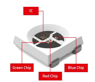
Figure 1: Illustration of the internal components of an ICLED (WE PN: 1315050930002)
The datasheet of an ICLED describes and summarizes the performance and technical characteristics of the products. As the ICLED differs from an “analog” LED, a new datasheet from Würth Elektronik with drawing specifications and performance graphs is introduced into the market. In addition to the information stated in the datasheet, Würth Elektronik provides this application note as a guideline on how to effectively read an ICLED datasheet from WE. Figure 2 introduces the first page of an ICLED datasheet (PN: 13150509030002). An overview of the order code, release date, drawing tolerances (norm) and the certifications of the product can always be found at the bottom center of each page of the data sheet.
The general structure of the ICLED datasheets is explained below:

Figure 2: First page of the 1315050930002 ICLED
Dimensions, recommended land pattern and pin configuration
The first section (Dimensions: [mm]) introduces a technical drawing of the selected PN. As the LEDs have different sizes and number of connections (pins), WE introduces the Recommended Land Pattern as a reference to create the footprint of the selected component in any PCB design software (e.g., Altium or Eagle). Regarding the stencil’s thickness, Würth Elektronik recommends a value of 120 µm. The pin configuration depicts the name of the pins corresponding to the soldering position of the ICLED (top view). An example of the presented drawing is shown on Figure 3. The ICLED requires both power supply and communication pins, therefore the naming of the pins is defined as:
VDD: This pin is used to supply power to the ICLED component (typ. +5 V).
VSS: The pin is connected to the ground or common reference of the power supply. It serves as the return path for the current flowing through the ICLED.
1. DIN (Data Input): This pin is responsible for receiving data signals that control the color and intensity of the ICLED. The data signal usually consists of a series of digital bits (1 or 0) encoded as a combination of logical levels (high and low) to specify the intensity values of the RGB LEDs within the package.
2. DOUT (Data Output): This pin is responsible for the transmission of the digital data to next ICLED connected in the circuit. The data output from one ICLED is connected to the DIN pin of the next ICLED (daisy chain connection).
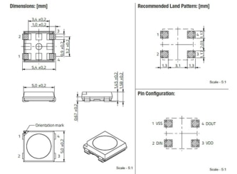
Figure 3: Dimensions (left),recommended land pattern (top right) and pin configuration (bottom left) of 1315050930002 ICLED
Absolute maximum ratings
The table depicted in Figure 4 indicates the absolute maximum ratings (input and output) of the ICLED to ensure proper usage, prevent damage, and maximize the lifespan of the component. Please note thatthe ICOutput Current (IF,IC) represents the current delivered from the IC to each individual R, G, B chip, this value is tested during the IC production process. However, as the IC itself is an active component, it requires energy to function properly. Nonetheless, the customer receives an enclosed package (IC with LED chips) these values cannot be measured individually. For this reason, the current to be measured on an ICLED consists of the operating current of the IC (IDD, ON) in addition to the IC output current. (IF, IC), as depicted in Figure 5. As previously mentioned, the value of the driving current is defined for one LED. In view of this, the maximum power dissipation is calculated by considering the total. current consumption of the LED. As the ICLED includes three chips, the total current consumption is tripled (the operating current of the IC ~1 mA is already included in the calculation).The maximum power dissipation of the LED is calculated as indicated by Equation (1):

Equation 1: Calculation of the total power dissipation of an ICLED
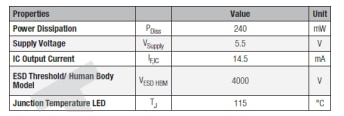
Figure 4: Absolute maximum ratings (PN: 1315050930002)
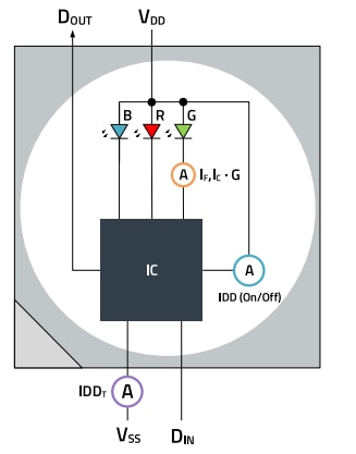
Figure 5: Differences on the ICOutput current (orange), IC operating current(cyan) and total current of an ICLED(magenta)
Packaging properties
This section covers the physical characteristics and specifications of the package in which the IC and LED chips are encapsulated. Information such as LED-chip technology, packaging specifications (PLCC or Chip LED), color of the packaging (only for PLCC ICLEDs) as well as the lens type (waterclear or diffused) can be found in the table shown in Figure 6. Note that independent of the LED model, the emitting color field refers to the order in which the LEDs light up in the communication protocol (e.g. GRB, RGB, BGR, etc.).

Figure 6: Packaging properties table
General information
From the information on the table below (Figure 7) the ambient conditions for operation and storage of ICLEDs is shown. Typically, the ICLEDs of WE operate at ambient temperature between -40°C and +85°C, in case operating temperature is outside the defined range it can lead to a reduced lifetime or even to complete failure of the component. Note that the Moisture Sensitivity Level (MSL) can be found at the end of the mentioned table. ICLEDs from WE are classified as MSL 31, meaning at least 168 hours of floor life after the original packaging has been opened.

Figure 7: General information table
Optical properties
The characteristics related to light emission of the individual R, G, B chips are presented on the table in Figure 8. The test conditions described next to the parameters indicate the voltage level (VDD) and the digital signal sent from the test microcontroller to the DIN pin of the ICLED. The capacitor (C) is included in the measurement process to prevent voltage drops and minimizing current spikes during the PWM control of the IC.
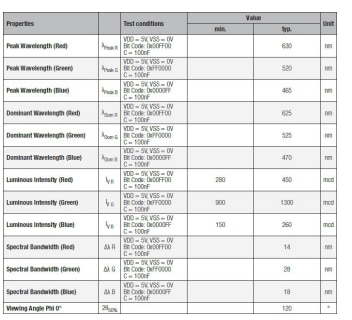
Figure 8: Optical Properties table
Electrical properties
The electrical properties table from Figure 9 define the operating boundaries of the ICLED. From the information on table, the operating supply voltage of the ICLED VDD is defined (typ. between 3.5 V and 5.5 V).
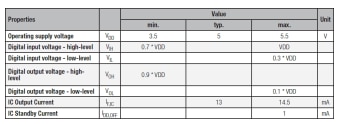
Figure 9: Electrical properties table
VIH and VIL specify the electrical requirements of the signal received through the DIN pin of the ICLED. Any input voltage greater than VIH is guaranteed to be recognized as a logic high state while any input voltage lower than VIL is guaranteed to be recognized as a logic low state. Typically, VIH and VIL are defined as a percentage of the operating supply voltage (VDD). According to the values of the table in Figure 9 and assuming an operating voltage of VDD = 5 V, can obtain the values for VIHmin and VILmax as indicated in Equation (2) and (3):

Equation (2): Calculation of VIHmin for VDD = 5V

Equation (3): Calculation of VILmax for VDD = 5 V
In case the supply voltage of the ICLED is not 5 V, the values for VIH and VIL should be calculated as explained before. VOH and VOL, on the other hand, refer to the voltage levels that determine the output levels of the signal transmitted from the DOUT pin of the ICLED. It is expected that the voltage level of a high logic state to be over VOH and when outputting a low logic level, the voltage value is lower than VOH. This ensures that the voltage levels of the output signal to be recognized by the subsequent ICLED connected in the circuit. The Figure 10 depicts a graphical representation of the voltage values that define the operation range of the ICLED.
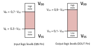
Figure 10: Graphicalrepresentation of the electrical operating boundaries of an ICLED
IF,IC describes the driven current from the IC to the individual LED chips and IDD, OFF corresponds to the operating current of the IC when all LED chips are turned off (PWM level of each chip equal to 0b0000000 or 0x00000) – also known as standby current.
Schematic of the ICLED
Würth Elektronik introduces an ICLED schematic depicted in Figure 11. This schematic depicts the internal connections between the IC and the LEDs chips and the order of appearance of the LED chips (from left to right) corresponds to the order in which these light up according to the communication protocol. In other words, there is no standard layout of the LED chips and depending on the manufacturer, the order of appearance changes (e.g., GRB as in the picture below, RGB, BGR, RBG, etc.)
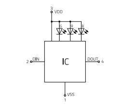
Figure 11: Schematic of an ICLED
Switching characteristics
The switching characteristics define the response time of the ICLED regarding the characteristics of the PWM signal, as well as the propagation delay of the output signal (with respect to the input signal). The parameters depicted on Figure 12 are briefly explained below: Assuming the following electrical operating values of an ICLED:

and

l LED chips and IDD, OFF corresponds to the operating current of the IC when all LED chips are turned off (PWM level of each chip equal to 0b0000000 or 0x00000) – also known as standby current. Schematic of the ICLED Würth Elektronik introduces an ICLED schematic depicted in Figure 11. This schematic depicts the internal connections between the IC and the LEDs chips and the order of appearance of the LED chips (from left to right) corresponds to the order in which these light up according to the communication protocol. In other words, there is no standard layout of the LED chips and depending on the manufacturer, the order of appearance changes (e.g., GRB as in the picture below, RGB, BGR, RBG, etc.) Figure 11: Schematic of an ICLED Switching characteristics The switching characteristics define the response time of the ICLED regarding the characteristics of the PWM signal, as well as the propagation delay of the output signal (with respect to the input signal). The parameters depicted on Figure 12 are briefly explained below: Assuming the following electrical operating values of an ICLED: VDD = 5V; VIH = VOH = VDD (4) and VIL = VOL = 0V (5)
1. tPLH [s]: Propagation delay where the input signal (DIN) crosses 50% of VDD to where the output signal (DOUT) crosses 50% of VDD when switching from low to high level.
2. tPHL [s]: Propagation delay where the input signal (DIN) crosses 50% of VDD to where the output signal (DOUT) crosses 50% of VDD when switching from high to low level.
3. tR [s]: Time interval of the rising edge of the PWM pulse (to one LED chip) from 10% to 90% of the pulse’s amplitude (VLED or VOUT RGB).
4. tR [s]: Time interval of the falling edge of the PWM pulse (to one LEDchip)from 10%to 90% ofthe pulse’s amplitude (VLED or VOUT RGB).
5. fPWM [Hz]: Frequency of the PWM signal that controls the single R, G, B chips.
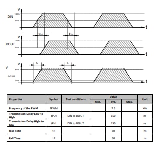
Figure 12: Input and output waveforms of an ICLED. Table indicates the typ. timing of the expected signals.
Data transfer time
The single wire communication protocol is formed by 24-bit data for each R, G, B LED. The data is formed by red, green, and blue data (not necessarily in this order), each with 8-bit width, and transferred with most significant bit (MSB) first. In case that two or more ICLED are daisy chained, the IC receives the first 24 bits of information and retransmits the remaining n-bits through the DOUT pin into the next ICLED. Each bit is recognized by a combination of both a high and a low logic pulse received through the DIN pin; the timing of these pulses defines if the IC recognizes the signal as a logical 1 or a logical 0. The logical bit 0 is represented by a pulse of length T0H with a high voltage level ≥ VIH and a pulse of length T0L with low voltage level ≤ VIL. Whereas a logical bit 1 is represented by a T1H with a high voltage level ≥ VIH and a pulse of length T1L with low voltage level ≤ VIL. In order for the ICLED to receive a new information package, a low pulse longer than Treset is required. The table depicted in the Figure 13 defines the timing required by the single wire communication protocol of the IC to distinguish between a logical bit 1, a logical bit 0 or a reset pulse.
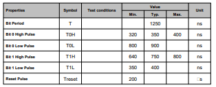
Figure 13: Data transfer timetable
Sequence chart
The Figure 14 provides a graphical representation of the single wire communication protocol. On the top part, the composition of the 24-bit data is depicted (e.g., GRB). As information of this communication protocol is sent with Most Significant Bit (MSB) first the data is transmitted from the leftmost bit (e.g., G7) moving towards the rightmost bit of each color data (G6, G5, G4… until G0). For illustration purposes, G7 and G6 are rewritten as 1 and 0 for the user of this datasheet to have a visual representation of the parameters that define the logical bit 1 and the logical bit 0 respectively. The graph on the bottom side of the figure represents the reset code (not to scale with the graphs for Bit 1 or Bit 0
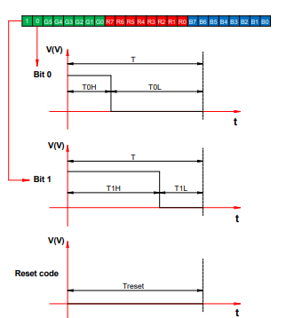
Figure 14: Graphical representation of the single wire communication protocol and the chip layout of an ICLED
Data transmission method
As the ICLEDs are designed to be daisy chained (by connecting the DOUT pin of one LED to the DIN pin of the next LED), Figure 15 illustrates the transmission of the information between an “N” number of ICLEDs
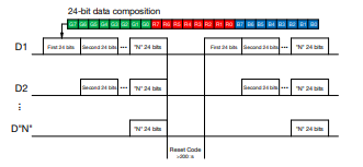
Figure 15: Representation of the data transmission method of SW ICLEDs
Define D1 as the information package sent from an MCU to the first ICLED, D2 is then the information package transmitted at the output of the first ICLED. D”N” is therefore the digital information transmitted at the output of the “N-1” ICLED in the chain. The figure illustrates that each time an ICLED receives a data package, the IC will reduce the information by 24 bits and retransmits the remaining ones into the next LED in the chain. A reset code should be read by the DIN pin of the first ICLED to indicate that a new information package is going to be transmitted.
Typical application circuit
The typical application circuit of an ICLED system is presented in the Figure 16, with the microcontroller (MCU) as the component that generates the data signals. This data signal is connected from the MCU to the DIN pin of the first ICLED, the rest components are then daisy chained. Würth Elektronik recommends the ICLEDs to be connected at VDD = +5 V and the addition of a bypass capacitor (C ~ 100 nF) as close as possible to the VDD pin of each ICLED to ensure a stable power and to block voltage fluctuations caused by the switch-on and switch-off currents of the ICLEDs. It is important to mention that this application circuit design may vary depending on the individual specifications/requirements from the customer’s application.
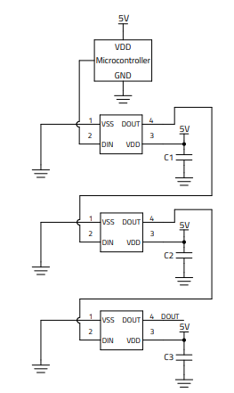
Figure 16: Typical application circuit of SW ICLEDs
Typical radiation plots of an ICLED
As a standard for WE, the graph presented in Figure 17 denotes the radiation pattern of an LED in both cardinal (left side) and polar coordinates (right side). The viewing angle of the LED is indicated by the FWHM angle or, in other words, where the intensity of the LED drops by 50%. For the 1315050930002 the viewing angle is then 120° (e.g., a Lambertian radiator).
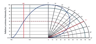
Figure 17: Viewing angle of an ICLED
The graph in Figure 18 provides the normalized emission spectrums of the single red, green and blue LED chips inside the ICLED (measured at PWM equal to 100%)
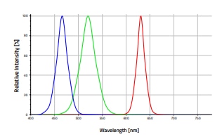
Figure 18: Spectral characteristics of the R, G, B LEDs inside the ICLED
Luminous intensity vs bit-code
As already mentioned, the R, G, B LED chips are controlled via PWM signal at a fixed current level. For this reason, the 256 brightness (8-bit) internal for each LED was subdivided and the luminous intensity values were performed at these selected subdivisions. The Figure 19 plots the typical luminous intensity of the single R, G, B LEDs against the 8-bit brightness selector of the corresponding color.
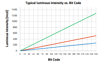
Figure 19: Dynamic plot luminous intensity (in mcd) vs 8-bit digital signal (for each color)
Packaging specification
The packaging specification consists of a detailed drawing of the tape and reel in which the LEDs can be ordered as indicated on Figure 20.
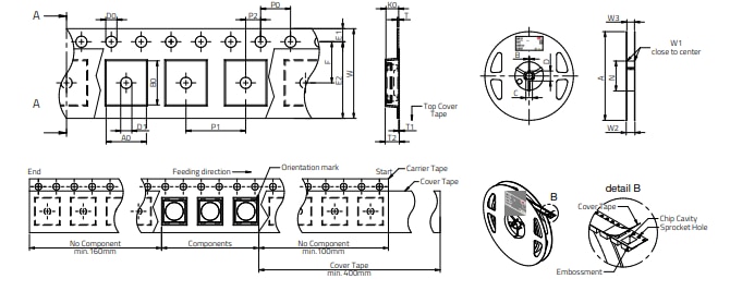
Figure 20: Tape and Reel-Specifications
A.1 References
[1] Editors: E. Barsoukov, J. R. Macdonald, Impedance Spectroscopy: Theory, Experiment, and Applications, Third Edition, John Wiley & Sons (2018)
[2] Luis Moura and Izzat Darwazeh, Introduction to Linear Circuit Analysis and Modelling: From DC to RF, Newnes an imprint of Elsevier (2005)
[3] B. E. Conway, Electrochemical Supercapacitors - Scientific Fundamentals and Technological Applications, Kluwer Academic Publishers, Springer, Boston (1999)
[4] A. F. J. Levi, Essential Classical Mechanics for Device Physics, Morgan & Claypool Publishers (2016)
[5] R. M. Hill and L. A. Dissado, Debye and non-Debye relaxation, Journal of Physics C: Solid State Physics, 18(19):3829-3836 (1985)
[6] D Edwards, J.-H Hwang, S.J Ford, T.O Mason, Experimental limitations in impedance spectroscopy: Part V. Apparatus contributions and corrections, Solid State Ionics, 99(1,2):85-93 (1997)
[7] Jong-Sook Lee et al., Impedance Spectroscopy Models for X5R Multilayer Ceramic Capacitors, Journal of the Korean Ceramic Society, 49(5):475-483 (2012)
[8] R. Kötz et al., Temperature behavior and impedance fundamentals of supercapacitors, Journal of Power Sources, 154:550–555 (2006)
[9] M. Schönleber, E. Ivers-Tiffée, Approximability of impedance spectra by RC elements and implications for impedance analysis, Electrochemistry Communications, 58:15-19 (2015)
[10] Bing-Ang Mei et al., Physical Interpretations of Nyquist Plots for EDLC Electrodes and Devices, The Journal of Physical Chemistry C, 122(1): 194-206 (2018)
[11] M.R. Hasyim, D. Ma and R. Rajagopalan and C. Randall, Prediction of Charge-Discharge and Impedance Characteristics of Electric Double-Layer Capacitors Using Porous Electrode Theory, The Electrochemical Society, 164(13): A2899-A2913 (2017)
[12] V. Srinivasan and J. W. Weidner, Mathematical Modeling of Electrochemical Capacitors, Journal of The Electrochemical Society, 146: 1650-1658 (1999)
[13] M. Itagaki, Electrochemical Impedance and Complex Capacitance to Interpret Electrochemical Capacitor, Electrochemistry, 75(8):649-655 (2007)
[14] T. Stolzke et al., Comprehensive accuracy examination of electrical power loss measurements of inductive components for frequencies up to 1 MHz, Journal of Magnetism and Magnetic Materials, 497: 166022 (2020)
[15] Online Manual, E5061B Network Analyzer, Keysight, URL: http://ena.support.keysight.com/e5061b/manuals/webhelp/eng/?nid=- 32496.1150148.00&cc=CA&lc=eng&id=1790874
[16] Data Sheet, E5061B Network Analyzer, Keysight URL: http://ena.support.keysight.com/e5061b/manuals/webhelp/eng/product_information/specifications.htm
[17] H.A. Wheeler, Formulas for the Skin Effect, Proceedings of the IRE, 30(9):412-424 (1942)
[18] A. E. Kennelly, F. A. Laws and P. H. Pierce, Experimental Researches on Skin Effect in Conductors, in Transactions of the American Institute of Electrical Engineers, 34(2):1953-2021 (1915)
[19] G. Schröder J. Kaumanns, R. Plath, Advanced measurement of AC resistance on skin-effect reduced large conductor power cables ,8th International Conference on Insulated Power Cables, Versailles – France (2011)
[20] E. Ivers-Tiffée and Aweber, Evaluation of electrochemical impedance spectra by the distribution of relaxation times, Journal of the Ceramic Society of Japan, 125(4):193-201 (2017=
IMPORTANT NOTICE
The Application Note is based on our knowledge and experience of typical requirements concerning these areas. It serves as general guidance and should not be construed as a commitment for the suitability for customer applications by Würth Elektronik eiSos GmbH & Co. KG. The information in the Application Note is subject to change without notice. This document and parts thereof must not be reproduced or copied without written permission, and contents thereof must not be imparted to a third party nor be used for any unauthorized purpose. Würth Elektronik eiSos GmbH & Co. KG and its subsidiaries and affiliates (WE) are not liable for application assistance of any kind. Customers may use WE’s assistance and product recommendations for their applications and design. The responsibility for the applicability and use of WE Products in a particular customer design is always solely within the authority of the customer. Due to this fact it is up to the customer to evaluate and investigate, where appropriate, and decide whether the device with the specific product characteristics described in the product specification is valid and suitable for the respective customer application or not. The technical specifications are stated in the current data sheet of the products. Therefore the customers shall use the data sheets and are cautioned to verify that data sheets are current. The current data sheets can be downloaded at www.we-online.com. Customers shall strictly observe any product-specific notes, cautions and warnings. WE reserves the right to make corrections, modifications, enhancements, improvements, and other changes to its products and services. WE DOES NOT WARRANT OR REPRESENT THAT ANY LICENSE, EITHER EXPRESS OR IMPLIED, IS GRANTED UNDER ANY PATENT RIGHT, COPYRIGHT, MASK WORK RIGHT, OR OTHER INTELLECTUAL PROPERTY RIGHT RELATING TO ANY COMBINATION, MACHINE, OR PROCESS IN WHICH WE PRODUCTS OR SERVICES ARE USED. INFORMATION PUBLISHED BY WE REGARDING THIRD-PARTY PRODUCTS OR SERVICES DOES NOT CONSTITUTE A LICENSE FROM WE TO USE SUCH PRODUCTS OR SERVICES OR A WARRANTY OR ENDORSEMENT THEREOF. WE products are not authorized for use in safety-critical applications, or where a failure of the product is reasonably expected to cause severe personal injury or death. Moreover, WE products are neither designed nor intended for use in areas such as military, aerospace, aviation, nuclear control, submarine, transportation (automotive control, train control, ship control), transportation signal, disaster prevention, medical, public information network etc. Customers shall inform WE about the intent of such usage before design-in stage. In certain customer applications requiring a very high level of safety and in which the malfunction or failure of an electronic component could endanger human life or health, customers must ensure that they have all necessary expertise in the safety and regulatory ramifications of their applications. Customers acknowledge and agree that they are solely responsible for all legal, regulatory and safety-related requirements concerning their products and any use of WE products in such safety-critical applications, notwithstanding any applications-related information or support that may be provided by WE. CUSTOMERS SHALL INDEMNIFY WE AGAINST ANY DAMAGES ARISING OUT OF THE USE OF WE PRODUCTS IN SUCH SAFETYCRITICAL APPLICATIONS.
DIRECT LINK
ANO009 | Understanding parameters in ICLED datasheets
USEFUL LINKS:
Application Notes : https://we-online.com/en/support/knowledge/application-notes
Services: https://we-online.com/en/products/components/service
Contact : https://we-online.com/en/support/contact
CONTACT INFORMATION
Würth Elektronik eiSos GmbH & Co. KG
Max-Eyth-Str. 1, 74638 Waldenburg, Germany
Tel.: +49 (0) 7942 / 945 – 0
Email: appnotes@we-online.de

