Application Note
Introduction to RF Inductors
ANP074 by Jose Martos & Dr. Heinz Zenkner
01. INTRODUCTION
RF inductors are used in a wide range of industries from consumer products to highly specialized scientific applications. RF inductors can be used in a plethora of functions in high frequency circuit design. These roles include circuit-tuning, impedance matching, filtering and even as high frequency chokes. One large market today is their use in wireless devices, such as tablets, but also in emerging products like IoT devices. Applications that are more specialized include radar, GPS and test equipment. Würth Elektronik eiSos offers a full range of RF inductors as part of the extensive portfolio of electronic components that are suitable for a wide range of frequencies and applications. Below we explain the most important characteristics of RF inductors, the different types and features of Würth Elektronik’s RF inductor series range, and some examples of applications in which they may be used.
02. CHARACTERISTICS OF RF INDUCTOR
In order to assess and compare the RF inductor series, it is necessary to understand in detail the main characteristics of an inductor for high frequency applications. Primarily, it must be remembered that RF inductors work exactly the same way as any other inductor. They are governed by the same physics rules that we see for power inductors. Therefore, we still characterize them in terms of their turns, permeability, inductance, and such parameters. Thus, the same formulas can be applied as they are with conventional inductors. Because of this similarity to power inductors, they both have very similar ranges of parameters which are visible in their datasheets, such as inductance (and its tolerance), DC resistance and rated current. However, we have some extra parameters, such as the quality factor, that are critical for the validation of RF inductors in a specific role. These parameters will be described below in greater detail.
2.1 Inductance Value and Tolerance
Since we are talking about inductors, the inductance is the most significant parameter. As with conventional inductors, this parameter is defined by the relative permeability of the core, cross sectional area of the core, the number of turns around the core and the effective magnetic path length of the core (Equation 1).
 (1)
(1)
L: Inductance [H]
µr: relative permeability
µo: free space permeability (4π·10-7 Vs/1 Am)
Aeff: effective cross-sectional area of the coil core [m2]
leff: effective path length in the coil core [m]
N: number of turns
The reason why most RF Inductors have a ceramic or air core is due to the needed low permeability in RF design, which allows high inductance stability, high Q factor and low losses, which are critical parameters in high frequency applications. Both ceramic and air have no magnetic properties, i.e. their relative permeability (µr) is ≈ 1 and thus do not influence the magnetic behavior of the inductor. According to the inductance equation of a coil, if µr ≈ 1 the inductance value can only increase with the number of turns or the dimensions of the inductor. This is the reason why RF inductors based on ceramic or air core only reach inductance values in the range of nH. Increasing the number of turns will also increase parasitic parameters which can reduce Q factor and the selfresonant frequency. In cases where larger inductance values in the range of µH are needed, ferrite cores (whose permeability µr > 1) are required as used in our series WE-RFI and WE-RFH.
In addition, in RF design, it is also very important to have tight inductance tolerances especially in applications such as filtering, matching and oscillator circuits. In other words, an RF inductor whose real inductance value is as close as possible to the nominal value is desired. This is the reason why many engineers appreciate narrower tolerances even if there is a reasonable extra cost. In the specifications, both the inductance value and tolerance are shown at a certain frequency point. In most RF applications like high order filters, oscillator circuits or impedance matching applications, it is very important that the inductance curve is as flat as possible over a wider frequency range (Figure 1), and in addition, the inductance value should be independent of the current.
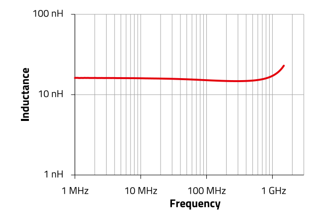
Figure 1 : Inductance curve of WE-TCI 0402 15 nH (744901115)
2.2 Self-Resonant Frequency
Because the winding structure of any coil of wire will exhibit some capacitance, the inductor will serve as a parallel resonant tank circuit with an associated self-resonance frequency (SRF). As with conventional inductors, SRF indicates up to which frequency the inductor behaves as an inductor. Exactly at the SRF the inductor with its parasitic capacitance behaves as a resonance circuit with an almost infinite high impedance, only circuit losses limit the high value of the impedance. Beyond the SRF the “inductor” behaves like a capacitor (Figure 2).
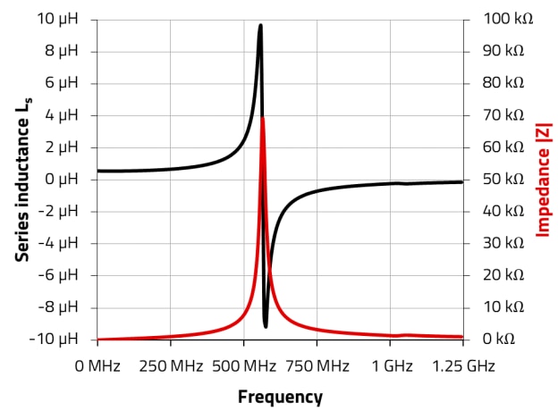
Figure 2: Inductance (L, black) and impedance (|Z|, red) of an inductor WE-RFH 1008 0.56 nH (744758256A)
As shown in the Figure 3, between the wires or internal electrodes of any inductor there is a distributed capacitance, which results in the equivalent circuit seen in Figure 4.
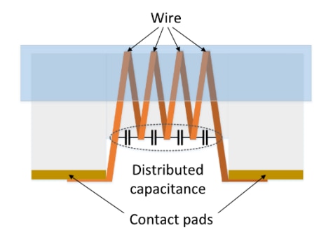
Figure 3: Schematic of a RF inductor. Parallel wires act like electrodes of a capacitor generating a distributed capacitance
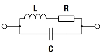
Figure 4 : Equivalent circuit of a RF inductor: L represents the inductance, R the losses of the wire and C the distributed capacitance
The relation between the inductance (L), the distributed capacitance (Cp) and the SRF is shown in the Equation 2:
 (2)
(2)
SRF: self resonance frequency [Hz]
L: Inductance [H]
Cp: distributed (resulting) capacitance [F]
Thus, the SRF is the frequency point at which the parasitic capacitance forms a parallel resonance with the inductance, or in other words, the frequency point where the capacitance is canceling out the inductance (i.e. both reactances are equal XL = XC). From Equation 2, it is also visible that increasing the inductance and/or the parasitic capacitance lowers the SRF, and vice versa. This is the reason why the larger the inductance value, the lower the SRF.
In case of choke applications in which inductors are used, the best signal blocking occurs shortly below the SRF, where the impedance is very high and thus the attenuation reaches its maximum. For filter or impedance-matching applications, it is more important to have constant inductance in the relevant frequency range, which means the SRF of the inductor should be well above the operating frequency of the circuit. A rule of thumb is:

A general tendency is the higher the inductance value, the lower the SRF, due to the increased winding capacitance of the inductor. Additional influences to the SRF are stray capacitances from the circuit, the components the inductor is connected to and the type of PCB used in the application. PCB-parameters like εr and laminate thickness decrease the SRF of the inductor. Furthermore, solder pads, circuit traces, ground and VCC planes influence it as well.
Some commercial design programs provide substratescalable inductor models, which allow implementing PCB material characteristics to a circuit simulation. Together with the S-parameters offered for each WE-RF-inductor the design can be simulated and calculated quite exactly. The S-parameters of the inductor describe accurately the properties of the component as a function of frequency, which account for all parasitic phenomena. Moreover, Würth Elektronik offers Modelithics models for most inductor series.
Modelithics consider the S-Parameters of an inductor on different substrate types and thicknesses, creating global models that scale the substrate-sensitive parasitic effects resulting in very accurate simulations. Although not always possible, it is best to solder the inductor into a design, which is as close as possible to the final product, and measure the circuit behavior in a set up with a network analyzer.
2.3 Quality factor Q
The quality factor Q is an essential characteristic parameter and one of the first things that every RF engineer should take into account. Depending on the manufacturer, the Q factor is given either as minimum or as typical value at a certain frequency point. In case of Würth Elektronik, the Q factor is given as the minimum value in order to guarantee to customers a reliable minimum level.
Basically, the Q factor is the ratio between the reactance XL and the losses RS and is an indicator of how ideal an inductor is (Equation 3). For inductors with air or ceramic cores, the resistance RS is mainly due to the resistivity of the conductor in the inductor device. A higher Q factor means less losses in the component.
 (3)
(3)
Q: Quality factor
XL: reactance [Ω]
RS: resistance [Ω]
L: inductance [H]
ω: angular frequency 2πf, f in [Hz]
Inductors with a ferrite core do not have a constant inductance L over frequency and the quality factor cannot be calculated simply by Equation 3. For a correct measurement of the quality factor, frequency-dependent real and imaginary losses of the ferrite material must be considered in the measurements along with the various inductance and capacitance effects of the inductor’s composite materials. A typical plot of the quality factor of a monolithic high-Q ceramic SMT inductor is shown in Figure 6. Figure 5 and Table 1 show the corresponding inductance curve and electrical data as given in the data sheet, Figure 7 shows the components themselves.
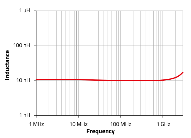
Figure 5 : Inductance graph
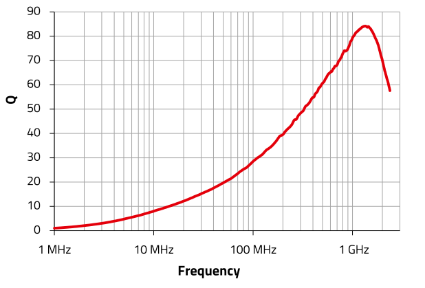
Figure 6 : Q-Factor-graph
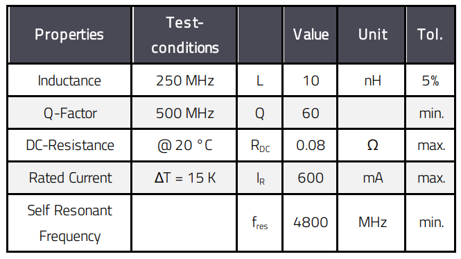
Table 1 : Electrical data of WE-KI SMT (744760110A)
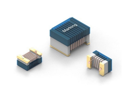
Figure 7 : High-Q SMD inductor with ceramic core WE-KI SMT Wire Wound Ceramic Inductor series
In wide band applications where inductors are needed to block a RF signal spectrum, it may be necessary to use an inductor with a ferrite core which can include considering the resistive part of the permeability of the ferrite. By using an inductor with a lossy ferrite core it may provide the attenuation impedance required across the desired frequency range. The tradeoff of this solution is that this component will contribute to the total losses of the circuit. Table 2 shows the electrical parameters of the WE-RFH Ferrite SMD Inductor. The diagram in Figure 8 shows the correlation between the quality factor Q, the DC resistance of the inductor and the reactance (XL).
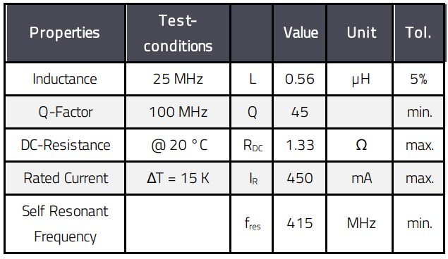
Table 2: : Electrical data of WE- RFH SMT (744758256A)
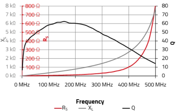
Figure 8 : Q factor (black), Inductive reactance (XL, grey) and Series resistance (RS, red) of an inductor WE-RFH 1008 (744758256A)
As mentioned, the DC-resistance of the wire is a parameter which influences to the losses and, therefore, to the Q factor of the inductor. The DC resistance is the most obvious contribution, but there are more effects which contribute to the Q factor of an inductor:
Skin effect: This influences the inductor’s Q factor because it raises the effective resistance of the wire with while increasing the frequency. The skin effect results from the tendency of an alternating current flow through the outer areas of a conductor rather than through the middle. This reduces the cross sectional area of the conductor through which the current can flow, thereby effectively increasing its resistance.
Core losses: In case the inductor uses a ferrite core, the ferrite material introduces losses as a result of various factors, each of which affects the inductor Q factor:
- Hysteresis losses: Magnetic hysteresis is an effect that causes losses due to energy consumption in the ferrite material. As ferrite materials are known for hysteresis losses, the effect on the inductor’s quality factor can be minimized by careful choice of the ferrite core material, and also ensuring that the magnetic field induced is within the electrical parameters of the core material specified.
- Eddy currents: Eddy currents are induced within the core of the inductor. Though they encounter higher resistance in the ferrite core, losses will occur and energy will be dissipated, thus the Q will be lowered. At the surface of the core eddy currents flow in phase with the coil current whereas induced currents inside the core are due to inductance out of phase.
Radiated energy: When an alternating current passes through the inductor, some of the magnetic field produced by the current will be radiated. Depending on the inductors shape and the construction of the ferrite core the radiated field may be small, but it still adds to the losses of the coil. In analogy to the resistance of an antenna the effect in the inductor is represented by a radiation resistance, too. Accordingly, this effect is a component of the inductor resistance and will reduce the inductor’s Q factor.
In summary, this means that, especially in the case of the Q factor, the user should select the parameters required for the application from the data sheet as Q is related to many other parameters of the inductor. REDEXPERT, the online tool of Würth Elektronik, is a very helpful tool to support the engineer in this manner (Figure 9).
2.4 DC-Resistance
RDC (or DCR) is the resistance of the inductor, specifically of the conductor. It describes one source of power losses of the inductor. Although for higher frequencies the losses are larger due to AC loss phenomena such as skin effect and proximity effect, the RDC is a good initial value to evaluate the losses of an RF inductor. Obviously, the RDC depends on the length and thickness of the wire. Thicker wire means lower RDC, but usually means increased dimensions of the component. Since the Q factor and the RDC, as a part of the total losses (RS), are inversely proportional (Equation 3), smaller RDC results in a larger Q factor. The RDC is defined in the specifications as the maximum possible value either in Ω or in mΩ.
2.5 Rated Current IR
The rated current IR is specified as the maximum DC current (A or mA) that causes a defined temperature rise (ΔT) (Figure 10). The mentioned ΔT depends on the series (in our case: ΔT = 15 K, ΔT = 20 K or ΔT = 40 K). The temperature rise plus the ambient temperature must not exceed the maximum operating temperature. In standard RF applications, the current is usually small, and therefore this parameter plays a secondary role.
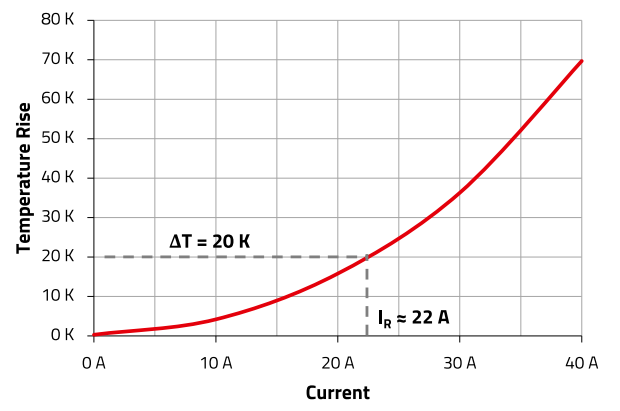
Figure 10 : IR- curve of an inductor WE-AC HC (7449152090)
Nevertheless, in applications where higher currents are required, Würth Elektronik offers a high current series for most of our inductor series (WE-KI HC, WE-AC HC and WE-RFH)
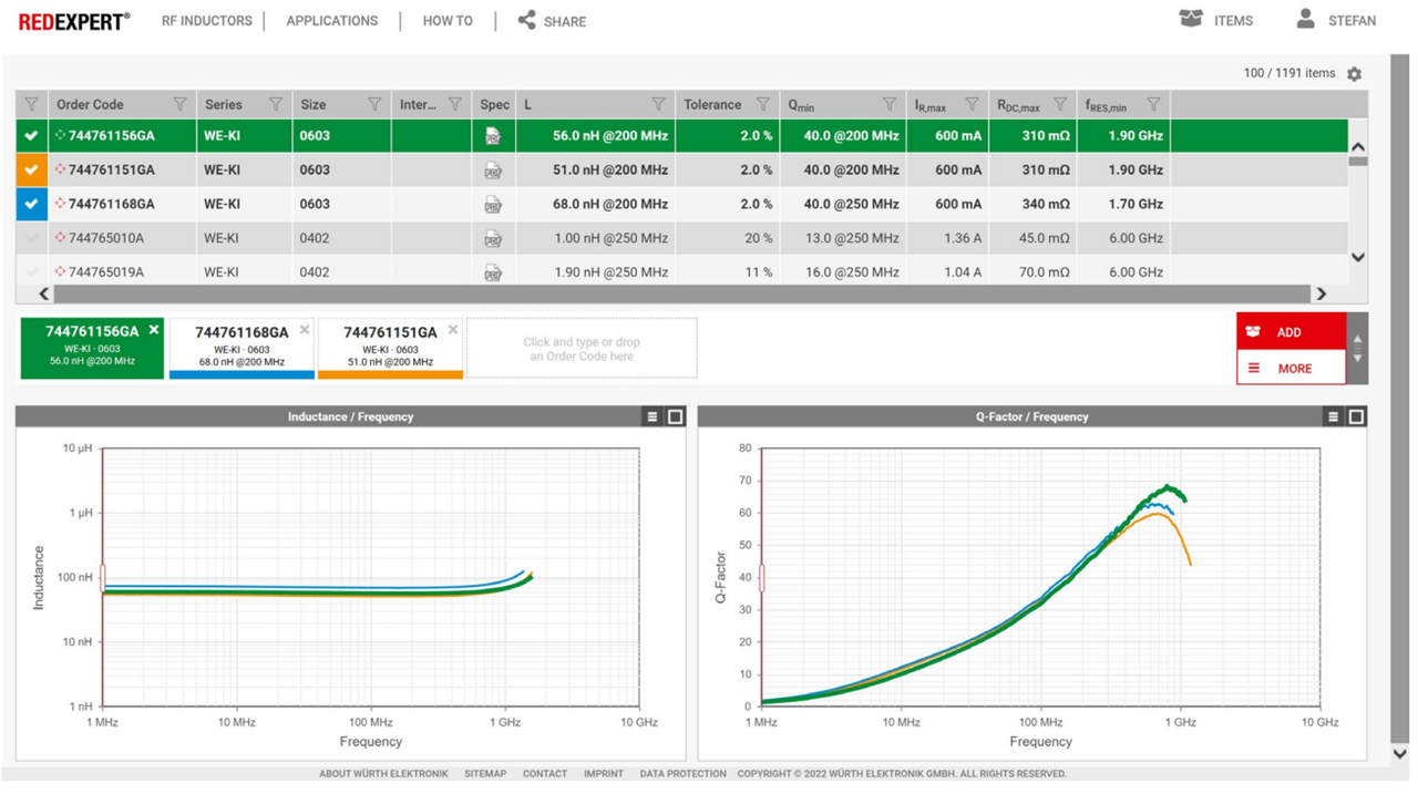
Figure 9: Comparison of different inductors WE-KI and the related electrical parameters in REDEXPERT
2.6 Size
Finally, in RF circuits size matters. In a market where eversmaller circuits are required, inevitably engineers place a lot of importance on this parameter. Würth Elektronik offers RF inductors from 0201 up to 1208 (inches), (Table 3). In the case of the air core inductors, the size is given in mm and it depends on the inductance value (i.e. number of turns). At this point, it is already obvious that all features are interrelated. For example, an inductor of size 0402 cannot have so many turns as an inductor of 0805, i.e. the maximal inductance value will be lower. In addition, smaller size means thinner wire, and that results in a larger RDC and lower Q factor. Therefore, engineers must take into account some trade-offs between sizes, performance and structure in order to select the right RF inductor for their application.
03. TECHNOLOGIES AND APPLICATIONS
3.1 Manufacturing Methods
Due to the frequency ranges that RF inductors need to operate in, a number of specialized materials and manufacturing techniques, which are not used in conventional inductors, are required.

Table 3: Sizes and inductance ranges of WE RF inductor series
Wire wound ceramic inductor
The structure of these inductors is a copper winding around a non-magnetic ceramic core. An epoxy top is added in order to enable the pick & place process.
The wire wound inductors use thicker wires which is the reason why the losses of this type of inductors are very low and therefore, we can achieve low RDC, very high Q factor and large rated currents. Wire wound ceramic inductors offer very good electrical parameters for a reasonable price. This is why this technology is very commonly used in most of RF applications.
With this type of technology Würth Elektronik offers two series: WE-KI and WE-KI HC. The difference between both series is that the WE-KI HC contains a thicker wire and therefore, the currents supported are higher and the Q factor slightly better than for WE-KI.
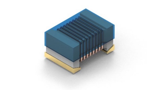
Figure 11 : Wire wound inductor
Wire wound ferrite inductor
Wire wound ferrite inductors consist in the same structure previously described but with a ferrite core. Since the ferrite has a high permeability, these inductors offer much higher inductance values than any ceramic inductor type.
Due to the thick wire, the wire wound ferrite inductors also offer high Q factor. However, the ferrite’s core losses increase for high frequencies. Therefore, the SRF is in the range of 500 MHz, which means that these inductors cannot be used in very high frequency applications. They can be usually found in noise filters such as in DC-DC converters
Würth Elektronik offers two series of wire wound ferrite inductors: WE-RFI and WE-RFH. The difference is again the thickness of the wire. WE-RFH has a thicker wire and consequently, a higher rated current than the WE-RFI.
Air core inductor
An air core inductor is just a coil of copper wire without any core. The only losses are due to the wire. Moreover, in order to keep the robustness of the structure, the wire must be very thick which results in extremely good electrical parameters.
This structure guarantees the highest rated current, the highest Q factor and the lowest RDC possible of all RF inductors. However, the number of windings is quite limited and, in consequence, the inductance values range is narrow. The air core inductors are mainly used in high frequency applications such as resonant circuits where low inductance values are sufficient.
Würth Elektronik has two air core inductor series: WE-CAIR and WE-AC HC. WE-CAIR’s structure is a round wire coil with an epoxy top to enable the pick & place. The WE-AC HC is the high current version of the air core inductors. Due to the flat wire and its dimension, they can support extremely high currents (typ. up to 40 A).
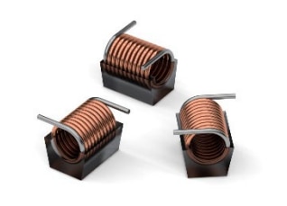
Figure 12 : Air core inductor
Multilayer ceramic inductor
These inductors are formed by layering ceramic sheets with printed electrodes. The electrodes are connected through vias forming a coil to create an integrated monolithic ceramic inductor. The multilayer ceramic inductor series of Würth Elektronik is called WE-MK.
In terms of price, this is the lowest cost technology. It offers a very wide range of inductance values and different sizes. Moreover, since there is less capacitive effect between electrodes, the SRF is very high. However, due to the thin electrode size, the multilayer ceramic inductors have higher RDC, lower rated current and lower Q factor as compared to wire wound inductors.
Thanks to the good overall balance, these inductors are suitable for many different RF applications such as RF matching, suppression of high frequency noise and mobile communication systems.
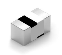
Figure 13 : Multilayer inductor
Thin film inductor
The thin film inductor consists of a coil printed on one thin layer of ceramic through a photolithographic process. Afterwards, the coil is covered forming the lowest profile and highly precise inductors. Thin film inductors offer high SRF and satisfactory values of Q factor. However, the number of turns of the printed coil is very limited and thus, the maximum inductance value is not as high as other technologies. Typical applications are in RF matching circuits or in any other RF application, where small inductor sizes at tight tolerance in inductance are needed.
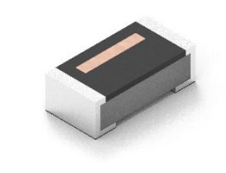
Figure 14 : Thin film inductor
In conclusion, each manufacturing method has its advantages and therefore, applications where they are best suited. As examples, below we will look at specific applications for Würth Elektronik’s range of RF inductors.
04. APPLICATIONS
The RF Inductors may be used in many different applications However, as described in the first chapters, for the proper function of the application, some points have to be considered, following the summary:
a. For tuned circuits like resonance circuits, filters, impedance matching circuits, a tight inductance tolerance is necessary.
b. Higher current requires a thicker wire to keep losses and temperature rise small. Larger wire lowers the RDC and increases the Q. However, the inductor will become larger and possibly have a lower SRF. Wire wound inductors have a higher rated current and a lower RDC than multilayer inductors of the same size and inductance value.
c. Higher rated current and lower RDC can be achieved by using a ferrite core inductor with less turns of wire. However, these inductors may show larger tolerances, lower Q, a larger variation of inductance over temperature and reduced saturation current ratings.
4.1 Colpitts Oscillator
At first glance, oscillators may appear to be inconspicuous circuits of an application. They are often simply purchased as finished components. However, they are no less important than other signal processing blocks, because without a bit clock there is no data transmission, without a clock signal no processor runs and without a carrier signal there is no radio. Where signals are digitized as fast as possible and then processed in a signal processor, the quality of the oscillator signals for sampling plays an essential role, similar role to that of a low-noise preamplifier. Every error in the current frequency is converted into signal errors during digital or analog conversion. The accuracy and stability of the generated frequencies is therefore a central design issue.
A resonant circuit becomes an oscillator when the losses occurring in the circuit are balanced by an amplifier so that the loop gain has the value 1. The total phase rotation at the resonant frequency must be 0° or 360°. Part of the oscillating circuit voltage must be fed back into the amplifier in phase.
If the capacitance in a parallel resonant circuit is split between two in series connected capacitors and the point between the capacitors is related to ground, then the two partial voltages at the capacitors are in phase opposition to each other. The following Figure 15 shows the signal conditions on the resonant circuit. The Figure 16 shows the voltages and the related phases at the capacitors.
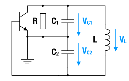
Figure 15 : Signal conditions on the resonant circuit
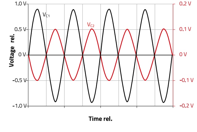
Figure 16 : Voltages and phases at the capacitors of a parallel resonant circuit with split parallel resonance capacitor
An oscillator with the capacitive divider and thus 3 capacitive connections is called a capacitive three-point oscillator or Colpitts oscillator according to its developer Edwin Henry Colpitts. In practice, Colpitts oscillators are realized with bipolar transistors or FETs as amplifiers because of the usually high oscillation frequency. These discrete circuits must then contain additional components for setting the operating point, as it is necessary with discrete amplifiers. The voltages at both ends of the L or C element are in phase opposition when resonant, since the tap is always connected to ground. This compensates the 180° phase shift of the transistor. The internal capacitances of the bipolar transistor (BJT) element itself are neglected by the phase condition and thus oscillation takes place at the resonant frequency of the parallel resonant circuit (Tank Circuit). The resonant condition can be calculated with following formula:
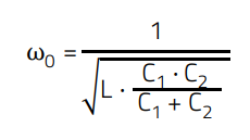 (4)
(4)
ω0: Angular frequency 2πf, frequency f in [MHz]
L: Inductance [H]
C1, C2: Capacitance [F]
The ratio of C1/C2 determines the feedback factor and must be compensated by the gain of the transistor, a practical relation is C1/C2 = 1:10. For higher frequencies (> 1/4 ft) the exact transistor parameters must be used to determine the resonance frequency and the feedback factor. ft is the transit frequency of the transistor, given in the data sheet. An analysis of the circuit is quite complex, therefore a simulation should be done with a simulation program. Simulations are not easy either, especially if the quality of the oscillating circuit is high, as the circuit must incorporate the real, lossy parameters of the components.
Schematic and Design Recommendations:
A Colpitts oscillator can be operated with a transistor amplifier in common emitter, base or collector circuit. The common base circuit should be used instead of the emitter circuit as the Colpitts oscillator in common base circuit has the advantage of decoupling the input and the output of the circuit. E.g. if the oscillator is in a critical circuit, like the tuning circuit of a receiver, the oscillator frequency cannot be coupled backwards into the antenna circuit and being radiated from there. Figure 17 shows an example of the oscillator in base circuit.
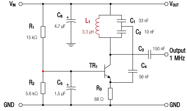
Figure 17 : Schematic of a 1 MHz Colpitts oscillator in common base circuit
Here the high-frequency feedback signal is conducted by the base capacitor C4 to ground. Phase rotation is not necessary because the common basic circuit amplifies without phase rotation. The feedback signal to the emitter is galvanicly decoupled from the operating voltage by the resonant circuit capacitors C1 and C2. The operating point of the transistor is set with a base series resistor or a base voltage divider and the emitter resistor.
Suitable RF Inductors
Table 4 shows the preferred component types in dependence of the oscillator frequency. Nevertheless, the other components of the circuit need to be selected accordingly.
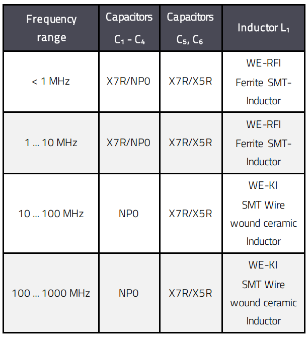
Table 4: Component types in dependence of the oscillator frequency
Capacitor types for resonance circuit up to 100 MHz:
WCAP-CSGP MLCCs (general purpose)
Capacitor types for resonance circuit above 100 MHz:
WCAP-CSRF MLCCs (HF purpose)
4.2 Biasing networks
The bias circuit is one of the most critical but often overlooked aspects of any RF circuit design. The bias network determines the operating point, i.e. the gain of the transistor over temperature as well as the RF control. The DC bias and thus the operating point of the transistor stage is determined independently of the RF design. Power efficiency, stability, noise and thermal behavior are the most important points when selecting a bias network.
The bias circuit supplies the DC voltage to the base, or to the gate of the transistor and thus determines the operating point. At the same time, the bias circuit must not influence the useful signal, which in most cases is also at the base of the transistor. In RF applications, the circuit must also be adapted to the system impedance.
Schematic and Design Recommendations
For good gain characteristics, it is necessary to bias the transistor with a collector current to reach the maximum transit frequency ftwith sufficient gain. Usually the manufacturer provides a curve in the data sheets for a bipolar transistor, which shows the transit frequency ft over the collector current IC. On the other hand, a low current IC is required for best noise performance. In order to correctly dimension the bias voltage and thus the collector current, i.e. the operating point, one must take into account the expected maximum signal level at the input of the transistor. The operating point must be at a sufficiently high current (and voltage) level to prevent the input signal from moving out of the "linear" operating range into the lower, curved range of the UBE/IC characteristic due to the collector current swinging out. Furthermore, the transistor must allow a sufficiently high operating current to prevent the input signal from driving the transistor into the saturated operating range. Both of the shifted operating states result in high signal distortion.
The BJT is often used as a low noise amplifier due to its low cost. With a minimum number of external matching networks, a BJT can be used to build a low-noise amplifier stage with high RF power, often better than a Monolithic Microwave Circuit (MMIC). Important for an RF BJT is that the variation in hFE (transistor gain) from transistor to transistor generally does not show as a difference in RF power. Two BJTs with very different hFE can still have similar RF power in the circuit as long as the transistors are at the same UCE and the collector current IC is equal due to the bias voltage UBE. This is the primary purpose of the bias network, i.e. keeping UBE and IC constant.
Figure 18 shows the schematic diagram of an amplifier stage in emitter circuit. The stage operates with voltage negative feedback (R1) and a bias network decoupled via inductors L1 and L2. Additionally, a current feedback with a resistor (R4) from the emitter to ground can be implemented to stabilize the transistor stage. This resistor can be bridged with a capacitor (C4) to maintain the AC voltage gain of the stage. The capacitor must have a low impedance in the signal frequency range.
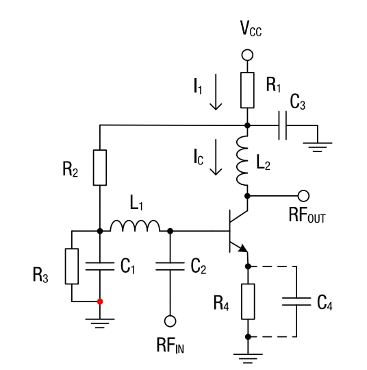
Figure 18 : HF transistor amplifier with current and voltage feedback and decoupled bias network
Suitable RF Inductors
Depending on the operating frequency and the required noise figure (decoupling), proper type of capacitors and inductors must be used. Table 5 shows the preferred component types in dependence of the operating frequency.
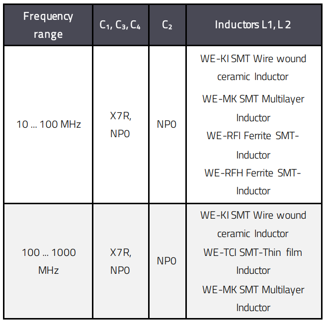
Table 5 : Component types in dependence of the operating frequency
The selection of inductors is critical. On one hand, the inductors must provide a sufficiently large impedance to decouple the DC circuits, and on the other hand they must not show any resonances in the signal frequency range.
The following inductors (Table 6), would be suitable for a small-signal amplifier stage in the frequency range from 400 to 500 MHz.

Table 6 : Recommended RF inductors in the frequency range from 400 to 500MHZ
The ceramic choke WE-KI 744761210GA with an inductance of 100 nH reaches an impedance of 250 Ω at 400 MHz, which is sufficient for most applications with a system impedance of 50 Ω. It is important that the maximum quality of the inductance does not coincide with the signal frequency range to avoid resonance phenomena. The curve in Figure 19 shows the quality Q of the inductance versus frequency. Alternatively, the high current ceramic SMT inductor WE-KI HC 744917210 can be used.

Figure 19 : Quality factor Q of the inductor WE-KI 744761210GA versus frequency
A ceramic multilayer inductor is the preferred choice for this application, like the WE-MK 7447840210, which offers the advantage of a lower quality and a reduced tendency to resonance. The rated current of this inductor is 150 mA, therefore the current IC should not exceed 60 mA - 80 mA for use in the collector circuit of the amplifier.
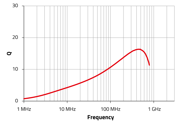
Figure 20 : Quality factor Q of the inductor WE-MK 7447840210 versus frequency
4.3 Passive filters and matching circuits
Passive filter circuits influence the frequency range of supplied electrical input signals. The circuits are called passive because the amplifying element, e.g. a transistor amplifier stage, is missing. Therefore, the output amplitude of passive filter circuits is always smaller or equal to the input amplitude. A passive filter has at least one characteristic passband and stopband, which can be described by the passband or attenuation behaviour. A cut-off frequency is defined for the transition range at which the amplitude of the output signal is attenuated by 3 dB. In EMC, preferably simple and combined low-pass filters are known. Combinations of simple low pass filters result in RC, LC, T- or π filters as shown in Figure 21 below. Filters can be built up from RC or LC combinations

Figure 21 : Various low-pass filters used in EMC
Only a few filter parameters are important in the EMC application area. These are the attenuation in the interference frequency range and, if necessary, the maximum current which can be driven through the filter. In the application area of filtering in the RF signal range, on the other hand, numerous other parameters such as edge steepness, selectivity (quality), phase delay and group delay are added to determine the filter properties. In order to achieve the requested level of these parameters, the components used, in particular the inductor, must be specifically selected. Some applications are discussed below to describe the topic of inductor selection.
It is not possible to realize a 1st order low pass filter with an LC element. A combination of L+C is always a 2nd order low pass filter. Higher order low-pass filters with RC elements are generally implemented as active filters. LC low-passes can be precisely adapted to the filter requirements by the specific property of the inductance. But LC-combinations tend to resonate and, if selected incorrectly, can lead to unwanted circuit problems.
4.4 Bias Tee (RF – DC – splitter for remote power supply)
The remote supply filter, the schematic is shown in Figure 22, separates a DC supply from HF signals. These filters are often used in antenna technology to supply preamplifiers or RFMixers remotely via the HF coaxial cable by a DC-supply which is contained in the local receiver
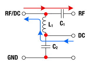
Figure 22 : Schematic of a Bias Tee network
In the upper circuit, the DC supply voltage is blocked towards the receiver by the capacitor C1. The high inductive impedance of L1 blocks the HF downwards, but is does not affect the DC current. The DC voltage is coupled in or out between C2 and L1 and is separated from ground by C2, while remaining HF signal is short-circuited to ground.
The above circuit was simulated with LTspice. The schematic of the simulation circuit is shown in Figure 23. The filter circuit consists of L1, C1 and C2. R1 and R3 are the system terminating impedances, V1 is the HF source with a signal level of 1V. V2 is a 12VDC source with an internal resistance of 5 Ω. For L1 a WE-KI SMT Wire Wound Ceramic Inductor 744760212A is used. The electrical parameters are shown in Table 7.
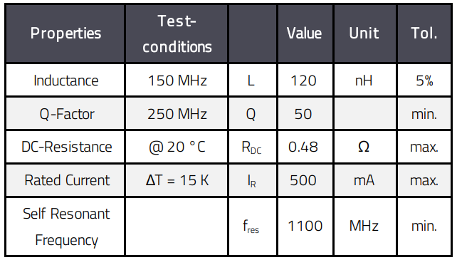
Table 7: Electrical parameters of the inductor WE-KI SMT Wire Wound Ceramic Inductor (744760212A)
The self-resonance frequency is above the highest HF-signal frequency. The maximum rated current is 500 mA, thus for being on the safe side and not to drive the inductor into saturation or over temperature the device connected to the filter at the HF_DC port should not have a current consumption above 400 mA.

Figure 23 : Schematic of the LTspice simulation set up of the filter shown in Figure 22
The diagram of the attenuation versus frequency of the ports UDC (V(UDC)), HF1 (V(HF1)) and HF_DC (V(HF_DC)) is illustrated in Figure 24.
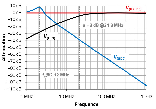
Figure 24 : Attenuation versus frequency of the ports UDC (V(UDC)), HF1 (V(HF1)) and HF_DC (V(HF_DC))
The HF_DC-port which carries the DC and the HF-signal is shown by the red trace. The HF-signal is linear over the whole frequency range. The HF-output signal at port HF1 has its 3 dB cut-off frequency point at 21.3 MHz and stays linear up to 1 GHz, which is more than sufficient for most wide band HF transmission. The UDC-port, supplied by V2 is effectively decoupled in the range above 3 MHz. But the diagram shows a resonance, up to 9 dB which is caused by the series resonance of L1 and C1. The resonance frequency of C1 and L1 can easily be calculated by
 (5)
(5)
With L1 = 120 nH and C1= 47 nF we get a resonance frequency of 2.12 MHz. In case there is no additional noise or signal in the signal path which would be affected by the resonance of the circuit which could be used like it is. In case of tendency to resonances caused by signals or interfering signals in the HF path, the ceramic inductor L1 must be replaced by another, preferably lossy inductor, e.g. a SMD ferrite inductor.
4.5 Resonance transformer Boucherot circuit
The Boucherot circuit is used to convert a system of constant voltage into a system of constant current. In the simplest case, it consists of a loss-free voltage resonant circuit, a simple LC filter as a series resonant circuit, which is operated in resonance with a load resistor connected in parallel to the capacitor, Figure 25 shows the circuit diagram. Like any transformer, this resonant transformer can transform both voltage and current, but has no electrical isolation and, moreover, works only in a narrow frequency band. It is therefore only used if the frequency does not change significantly. Circuits with the resonance transformer are for example found in electronically controlled fluorescent tubes, in energy-saving lamps and in cold cathode tubes for the backlighting of TFT-LCD flat screens. In high-frequency technology and in transmitters and receivers, power matching between different function blocks, to the antenna and to different cable impedances can be achieved by means of resonance transformers.
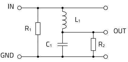
Figure 25 : Schematic of the resonance transformer or the Boucherot circuit
In order to determine the values of inductor L1 and capacitor C1 for power matching, the impedances of the resonance transformer on both sides must correspond to the values of the two resistors R1 and R2 respectively. The dimensioning can be done either graphically with a Smith chart or mathematically within the framework of the complex alternating current calculation. The two formulas for L and C, which are stated in literature are as follows.
 (6)
(6)
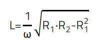 (7)
(7)
C: Capacitance [F]
L: Inductance [H]
ω: Angular frequency 2πf, f in [MHz]
Rx: Resistances [Ω]
The following example shows the adaptation of a 75 Ω transmission system to a monopole antenna, simulated with LTspice. A monopole antenna has at λ/2 a base point impedance of approx. 2,500 Ω, the transmission system in the example was assumed to be 75 Ω. The signal level at the input is 1 V, the operating frequency is 100 MHz. The simulation set up is shown in Figure 26.
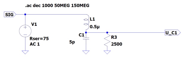
Figure 26 : LTspice-set-up of the resonance transformer
Due to the formula above the values for the components L1 and C1 are C1 = 3.6 pF and L1= 0.68 uH. Simulated with this value the resonance of the transformer is approx. at 79 MHz. A simulation result with the values given in the schematic of Figure 26 is shown in Figure 27.
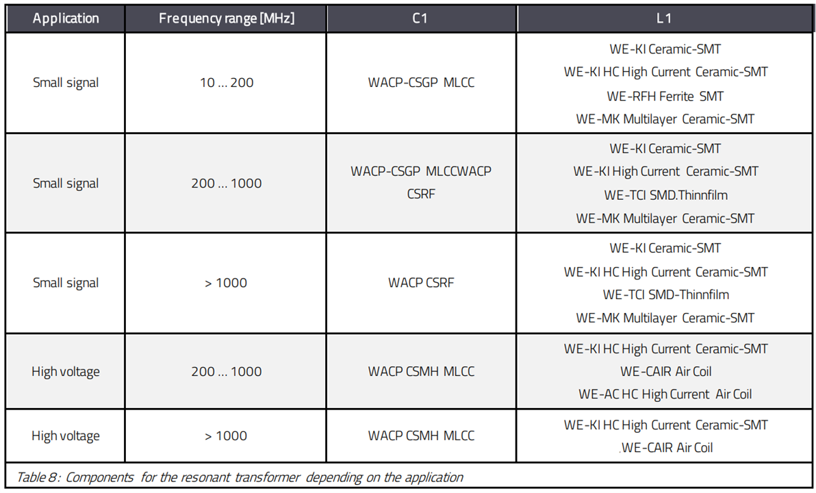
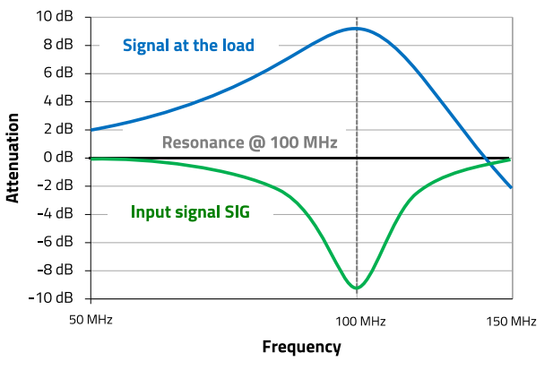
Figure 27 : Resonance transformer simulation according to schematic in figure 26
The values for the resonance circuit are L1 = 0.5 uH and C1 = 5 pF. At resonance the voltage at the capacitor C1 and thus at the load R3 increases up to approx. 9 dB, which is about 2,8 V. The components used in this resonance circuit are critical. As can be seen, the voltage level at the capacitor increases in dependence of the impedance and in cases where the voltage level is already high at the source (e.g. 100 V) the rated voltage of the capacitor C1 must be high as well, in the case of the example > 300 V. Furthermore, the components should have a high quality and low losses to achieve high efficiency and low insertion loss. This means the RDC of L1 must be low and the Q of the capacitor high. The Table 8 gives an overview about selections of components in dependence of the application.
4.6 Impedance Matching of a WiFi antenna ports
To adapt a HF source to a load, the Boucherot resonance transformer can be used, as described in section 4.5. The lower the impedances of the source and load impedance differ, the lower the quality of the circuit and the wider the bandwidth of the resonance transformer. In this case, two differently dimensioned LC low-pass filters can be connected together to form a π filter. The filter allows impedance matching between source and load even for higher quality values. In the following example, the circuit was used to adapt a WiFi transceiver to a hybrid antenna. Figure 28 shows the schematic of the antenna-matching circuit.
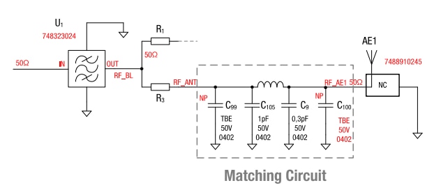
Figure 28 : Schematic of the transceiver-antenna matching circuit
The RF signal from the transceiver first reaches a band pass before it is routed either to antenna port 1 or antenna port 2 via an alternatively equipped 0 Ω resistor. C105 and C9 together with L3 form the π low pass filter for matching the hybrid antenna. C99 and C100 are additionally available placement positions which can be used for fine tuning.
Figure 29 shows the corresponding layout.
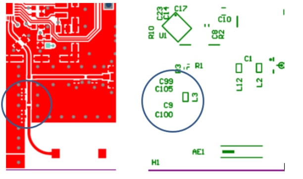
Figure 29 : Layout of the transceiver-antenna matching circuit related to the schematic in Figure 28
If matched, at operating frequency, maximum power transmission should be achieved and the attenuation outside the bandwidth should be as high as possible. The matching was in this case performed with a network analyzer. The measured parameter for matching is the reflection loss S11. If a reflection in the signal path happens, a part of the signal, coming from transmitter is reflected because of the different impedances between the transceiver and the antenna. Since the impedance is generally frequency dependent, this means that the reflection is also frequency dependent. The smaller the impedance differences are, the smaller the reflections are. With identical impedances, no reflections occur.
The reflection loss is specified in decibels (dB) and is the logarithmic ratio between the reflected signal and the input signal. The greater the reflection loss, the better the impedance matching of the components. The WiFiTransceiver operates in the range of 2.45 GHz. The matched component values with the corresponding chart of the reflection loss S11 is shown in Figure 30.
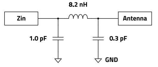
Figure 30 : Antenna Matching circuit
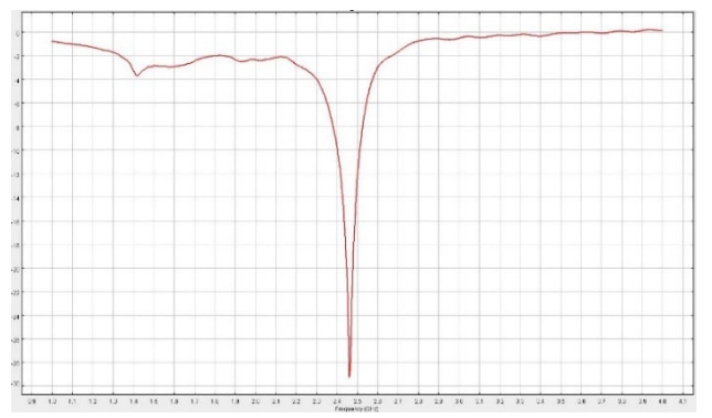
Figure 31 : Matched component values with the corresponding chart of the reflection loss S11
Figure 31 shows, that at the operating frequency the reflection loss is approx. 29 dB, which is a good value, VSWR is then approx. 1.06.
Applications in this frequency range require very low-loss components, especially in the operating mode of HFtransmission. Each dB attenuation in the transmission path means loss of transmission energy that must be compensated with higher transmission power, which generally also means a higher proportion of harmonics in the transmission signal. In the following Table 9 the components used for the filter are listed
Table 9: Components used for the filter, according to schematic in Figure 30 4.7 VCOs The voltage-controlled oscillator (VCO) is an electrical oscillator whose frequency can be changed by the magnitude of an applied voltage (control voltage). The design of a VCO depends essentially on the operating frequency and the required adjustment range. The VCO must exhibit a low phase noise in order to meet the sensitivity, adjacent channel and blocking requirements. In digital modulation scheme, the VCO’s phase noise affects the bit error rate (BER) requirements. A change of the oscillation frequency with supply voltage can cause phase noise degradation due to
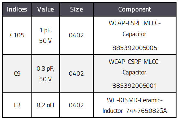
Table 9: Components used for the filter, according to schematic in Figure 30
4.7 VCOs
The voltage-controlled oscillator (VCO) is an electrical oscillator whose frequency can be changed by the magnitude of an applied voltage (control voltage). The design of a VCO depends essentially on the operating frequency and the required adjustment range. The VCO must exhibit a low phase noise in order to meet the sensitivity, adjacent channel and blocking requirements. In digital modulation scheme, the VCO’s phase noise affects the bit error rate (BER) requirements. A change of the oscillation frequency with supply voltage can cause phase noise degradation due to increased sensitivity to the power supply noise. VCO output power in dBm is usually defined into a 50 Ω load. The tuning slope is the analogy of the frequency to the voltage tuning characteristic. With an increasing VCO frequency range, it is difficult to achieve flat output power increase. Therefore, adding an output filter to suppress harmonics in some cases may degrade power output flatness. The drive level should consider the trade-off between harmonic content, oscillator stability, and noise.
Schematic and Design Recommendations:
Oscillator design specifications often require a given output power into a specified load over the specific frequency range. In the circuit in Figure 32, the supply voltage and bias current determine the operating point of the transistors. The oscillator frequency is determined by the resonance components. The selection of the transistor should consider noise, frequency, and power requirements. Based on the particular component, the design may need to consider parasitics of the specific resonator components. The VCO schematic presented below in Figure 32 uses the Infineon low noise RF transistor BFP420. In order to minimize the phase noise, the Q of the tuned circuit in the oscillator must be maximized. A low Q-factor of an LC tank and its component tolerances needs careful design for phase noise without individual readjustment of the oscillators. Noisy power supplies may cause additional noise which may be seen at offsets in the range from 20 Hz to 1 MHz from the carrier frequency. The phase noise performance of the VCO may degrade depending upon the type of regulator used. To improve the phase noise performance of the VCO a low noise DC-DC converter design, RF chokes and good bypassing capacitors (low ESR) are recommended.
In the schematic below, the differential transistor pair Q1 and Q2 represents, due to positive feedback, a negative resistance to the resonator circuit. The negative resistance cancels the losses of the resonator, enabling sustained oscillation. With the two varicap diodes D1 and D2 the frequency can be varied. By implementing the filter with L3 and C5 the noise of the signal can be reduced effectively. The inductor L3 and capacitor C5 form a 2nd order low-pass filter which prevents noise at even harmonics from being injected into the feedback path of the oscillator. Additionally, the phase noise degradation due to a noisy control voltage V_varicap is very significant at the lower frequency range where the varicap diodes are most non-linear.
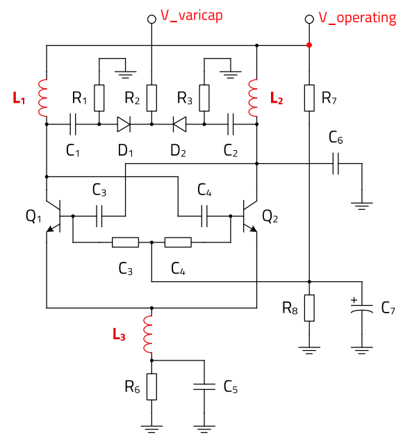
Figure 32 : Schematic of a voltage controlled oscillator (VCO) for the frequency range between 500 MHz and 1 GHz
Suitable RF Inductors:
WE-KI and WE-KIHC series would be a good option due to their excellent Q-Factor and tight inductance tolerance offered.
05. OVERVIEW
In this application note the essential parameters of RF inductance were explained and further deepened with common applications. Significant differences between an RF inductors and a power inductors were pointed out. While it is important for power inductors to have a high impedance, a high nominal current and a high saturation flux density, quality and resonance frequency are the essential parameters for RF inductors. For this reason, the Q-factor is a fundamental property of RF inductors. It was pointed out, that all parameters of an RF inductor are interrelated and therefore, trade-offs between sizes, performance and RF characteristics must be considered. Depending on the application and the function of the inductor in it, specific features become more important over the others.
Würth Elektronik has a wide RF inductor portfolio with series in all the described technologies. Moreover, in each series there are available plenty of sizes, different inductance and tolerance values in order to find the best suitable RF inductor for your application. In addition, in the REDEXPERT tool a great support in the selection of the RF inductors can be found. All needed parameters and curves of WE RF inductors can be found and compared, so that the selection is fast, simple and efficient.
IMPORTANT NOTICE
The Application Note is based on our knowledge and experience of typical requirements concerning these areas. It serves as general guidance and should not be construed as a commitment for the suitability for customer applications by Würth Elektronik eiSos GmbH & Co. KG. The information in the Application Note is subject to change without notice. This document and parts thereof must not be reproduced or copied without written permission, and contents thereof must not be imparted to a third party nor be used for any unauthorized purpose. Würth Elektronik eiSos GmbH & Co. KG and its subsidiaries and affiliates (WE) are not liable for application assistance of any kind. Customers may use WE’s assistance and product recommendations for their applications and design. The responsibility for the applicability and use of WE Products in a particular customer design is always solely within the authority of the customer. Due to this fact it is up to the customer to evaluate and investigate, where appropriate, and decide whether the device with the specific product characteristics described in the product specification is valid and suitable for the respective customer application or not. The technical specifications are stated in the current data sheet of the products. Therefore the customers shall use the data sheets and are cautioned to verify that data sheets are current. The current data sheets can be downloaded at www.we-online.com. Customers shall strictly observe any product-specific notes, cautions and warnings. WE reserves the right to make corrections, modifications, enhancements, improvements, and other changes to its products and services. WE DOES NOT WARRANT OR REPRESENT THAT ANY LICENSE, EITHER EXPRESS OR IMPLIED, IS GRANTED UNDER ANY PATENT RIGHT, COPYRIGHT, MASK WORK RIGHT, OR OTHER INTELLECTUAL PROPERTY RIGHT RELATING TO ANY COMBINATION, MACHINE, OR PROCESS IN WHICH WE PRODUCTS OR SERVICES ARE USED. INFORMATION PUBLISHED BY WE REGARDING THIRD-PARTY PRODUCTS OR SERVICES DOES NOT CONSTITUTE A LICENSE FROM WE TO USE SUCH PRODUCTS OR SERVICES OR A WARRANTY OR ENDORSEMENT THEREOF. WE products are not authorized for use in safety-critical applications, or where a failure of the product is reasonably expected to cause severe personal injury or death. Moreover, WE products are neither designed nor intended for use in areas such as military, aerospace, aviation, nuclear control, submarine, transportation (automotive control, train control, ship control), transportation signal, disaster prevention, medical, public information network etc. Customers shall inform WE about the intent of such usage before design-in stage. In certain customer applications requiring a very high level of safety and in which the malfunction or failure of an electronic component could endanger human life or health, customers must ensure that they have all necessary expertise in the safety and regulatory ramifications of their applications. Customers acknowledge and agree that they are solely responsible for all legal, regulatory and safety-related requirements concerning their products and any use of WE products in such safety-critical applications, notwithstanding any applications-related information or support that may be provided by WE. CUSTOMERS SHALL INDEMNIFY WE AGAINST ANY DAMAGES ARISING OUT OF THE USE OF WE PRODUCTS IN SUCH SAFETYCRITICAL APPLICATIONS
DIRECT LINK
ANP074 | Introduction to RF inductors
USEFUL LINKS:
Application Notes : https://we-online.com/en/support/knowledge/application-notes
Services: https://we-online.com/en/products/components/service
Contact : https://we-online.com/en/support/contact
CONTACT INFORMATION
Würth Elektronik eiSos GmbH & Co. KG
Max-Eyth-Str. 1, 74638 Waldenburg, Germany
Tel.: +49 (0) 7942 / 945 – 0
Email: appnotes@we-online.de

