Application Note: WE-RJ45 LAN for Through-Hole Reflow

ANP078 BY JEFFERY LIU
1 Introduction
Through-Hole Reflow (THR) technology is a process in which throughhole components are soldered to a printed circuit board (PCB) by using reflow technology. It allows soldering the through-hole components and surface-mount components at the same time and with the same reflow profile. This makes the process more cost effective and saves time, as no wave soldering is needed anymore. Through-Hole Reflow is becoming more and more popular, not only for EMS (Electronic Manufacturing Services) companies, but also for customers with smaller production lines.
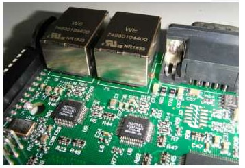
Figure 1: Demo board
2 Features and benefits of WE-RJ45 THR
The main requirement of the through-hole components is to withstand high temperatures during reflow soldering. Here not only the plastic housing material must be seen, but also the LEDs, where chip and leadframe are ofter sensitive for high temperatures. A further design requirement is to make sure the reflow heat can reach all solder points in the same way and with the same result. A final requirement to be considered is the component handling with pick and place equipment. With the correct modifications of the assembly process, the manufacturer can ensure the quality and long term reliability of the solder joint. In this section, we will clarify which design aspects had to be improved or changed in order to obtain good results with our WE-RJ45 THR connectors.
2.1. Housing material
In current through-hole connectors, the plastic used for the housing is Nylon or PBT (polybutylene terephthalate). As the melting point of these materials is 220 °C (Nylon) and 223 °C (PBT) respectively, they can withstand short periods of high temperature at wave soldering. But with 20 seconds holding time over the liquidus temperature (217 °C) these materials cannot withstand reflow soldering temperatures during reflow soldering. Thus, LCP (Liquid Crystal Polymer) is commonly chosen for reflow soldering, as it has a high melting point (330 °C) and low humidity absorption.
2.2. Stand-off of housing
A THR component is characterized by a standoff between PCB and component in order to allow a better air flow between the connector and the PCB. Furthermore, it provides enough space for the solder paste. In addition, the construction of the component‘s housing should allow an Automatic Optical Inspection (AOI) of the solder joint and ensure that there is no contact with the solder paste during reflow. Normally, the stand-off for RJ45 connectors is 0.50 mm. However, in order to improve the solderability results, Wurth Electronics has designed the THR RJ45 connectors with 1.20 ~ 1.60 mm stand-off. See figure 2.
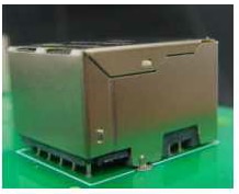
Figure 2: Stand-off
2.3. Pin length
Another important aspect of the RJ45 connectors for IR reflow soldering process is the pin length. If the pins are too long, the distance between the solder paste and the PCB will be too large, creating solder balls on the pins’ head and providing poor soldering results (see figure 4). Too short pins will sink into the PCB. The soldering spots will be good, but the solderability results will not fulfill the IPC-A-610 criteria (see figure 3). Ideally, the pins should come out from the PCB between 0.20 mm and 0.80 mm, in order to achieve good soldering results. The pin length of the WE-RJ45 THR is 2.20 mm, making it compatible with a PCB thickness of 1.40 ~ 2.00 mm (figure 5).

Figure 3: Comparison of soldering with different pin lengths
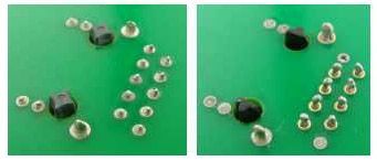
Figure 4: Perfect soldering result with visible meniscus on the left and poor soldering result with solder balls on top of the pins due to pin length
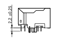
Figure 5: The pin length of the WE-RJ45 THR is 2.20 mm, which makes it suitable for a PCB thickness of 1.40 ~ 2.00 mm
2.4. Connector type
Not all RJ45 connector types can be used for THR, even if the right material, stand-off and pin length are used. For some existing designs and under normal operations, the solder temperature will not melt the solder paste in the pin holes. From experience, solder joints that are distance of more than 1 mm away from the RJ45s outer edges will not solder properly as the paste is not melted by the reflow heat completely.
3 How to use THR products
The reflow process should produce acceptable through-hole solder joints that comply with IPC standard. The joints should have no voids and produce a fillet (see figure 6).
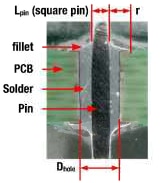
Figure 6: Illustration of a proper through-hole solder joint
Following design steps have to be considered carefully:
- PCB layout
- Stencil design
The stencil should ensure that the appropriate quantity of the solder paste can be printed onto the through-hole to achieve an excellent solder joint after reflow.
- The printing process should be optimized
- The reflow profile should be compatible with SMT components
3.1. PCB layout
The hole diameter should be measured including the plating. If the PCB hole diameter is too small, it is very difficult to mount the component onto the PCB and less solder volume in a small hole can cause an unsufficient connection between pin and PCB. On the other hand, an oversized hole can cause less meachincal stability of the part before reflow soldering. Additionally, larger holes require more solder. We recommend a hole design as Figure 7. A recommended land pattern is given in all Würth Elektronik THR datasheets as may be seen in Figure 8.

Figure 7: Design rule for the diameter of the PCB hole Dhole = Dpin + 0.3 mm
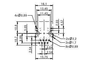
Figure 8: Recommended land pattern from datasheet WE-RJ45 THR 749 801 044 00
3.2. Solder paste volume calculation
Before designing the stencil, the volume of solder paste should be calculated to decide the aperture and thickness of the stencil. Approximately, half (50 %) of the solder volume is metal. The other 50 % is flux, which oozes out during reflow process. To get enough solder for pads and holes, the double amount of solder paste should be used. The total volume of the solder paste (Vpaste ) is calculated by the hole volume (Vhole ) minus the pin volume (Vpin )and add the fillet volume (Vfillet) for top and bottom sides. The formula is,
Vpaste = 2 (Vhole - Vpin + 2 ⋅ Vfillet ) Eq.(1)
Vhole = π 4 ⋅ Dhole 2 ⋅ T Eq.(2)
Vpin = Lpin ⋅ Wpin ⋅ T Eq.(3)
Vfillet = 0.215 ⋅ r2 ⋅ 2 π ⋅ (0.2234 ⋅ r + 1 2 Wpin) Eq.(4)
Where:
Dhole Diameter of hole
Lpin Length of pin
Wpin Width of pin
T Thickness of PCB
r Radius of fillet
Example to calculate the volume of solder paste for 74980104400
Pin size: 0.40 mm x 0.40 mm
Suggested PCB hole size: Ø 0.89 mm
PCB thickness: 1.60 mm
Diameter of soldering PAD: 1.40 mm
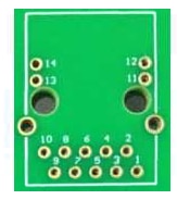
Figure 9: PCB layout
According to equation (2)
Vhole = π 4 ⋅ (0.89 mm)2 ⋅ 1.6 mm = 0.9954 mm3
Following equation (3)
Vpin = 0.4 mm ⋅ 0.4 mm ⋅ 1.6 mm = 0.256 mm3
As per equation (4)
Vfillet = 0.215 ⋅ [(1.40 - 0.89) mm] 2 ⋅ 2 ⋅ 3.14 ⋅…
… [0.2234 ⋅ (1.40 - 0.89) mm + 1 2 ⋅ 0.4 mm] = 0.110 mm3
Applying equation (1), we obtain
Vpaste = 2 (0.9954 mm3 - 0.256 mm3 + 2 ⋅ 0.110 mm3 )
Vpaste = 1.9188 mm3
3.3. Stencil design
Stencil design is an important element in the through-hole reflow process. The stencil must deliver the correct amount of solder paste to the through-hole during the stencil printing process. The area of the stencil aperture is determined by the requested solder volume. The aperture can be either a rectangle, circle or any other form. The most important factor is to get enough paste for soldering. For example, if the thickness of stencil is 0.15 mm, then the area of aperture should be:
Saperture = (1.9188 mm3 - 0.9954 mm3) / 0.15 mm = 6.15 mm2 Eq.(5)
Here, the volume of hole should be subtracted, since it was filled after printing. So, we can design the cutoff of the stencil as 2.20 mm 2.80 mm = 6.15 mm². A recommended stencil layout for a stencil thickness of 0.15 mm is integrated into all WE-RJ45 THR datasheets like in figure 10.
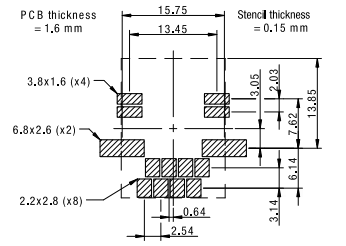
Figure 10: Recommended stencil design from datasheet WE-RJ45 THR 749 801 044 00
3.4. Printing
There are different methods how the solder paste can be applied to the PCB for THR. In difference to regular SMT process, pads and also the pin holes need to be filled with solder. In order to reach that, it needs to make sure that the solder is pressed into the holes properly. This can be done with one or more than one step:
- Printing twice
At the first step, the solder paste is applied from the PCB top side. For the second printing step, no additional solder paste will be used. Instead, the solder paste of the first time printing will be pushed deeper into the drilling holes.
- Printing with different stencils.
Another method is that two stencils are used. The first stencil applies solder for the drill holes (not for the pads around). The second stencil applies solder to the drilling holes and the solder pads. In difference to “printing twice” solder is applied to the PCB in both printing steps. The second step can also be used to place solder paste for other SMT components on the PCB. For our tests with RJ45 LAN transformers, we didn´t evaluate this method.
- Stencil with etched recesses
A further solution is to use a stepped stencil. A first stencil is used to apply solder to all SMT components. The stepped stencil is used in a second step to apply solder to the THR drilling holes plus their solder pads. On its bottom side it has etched recesses, so that the already soldered pads of the SMT components are prevented from blurring. For our RJ45 parts we calculated a minimum thickness of 0.15 mm of solder to be applied on the drilling holes. If other SMT components should be soldered with 0.1 mm solder thickness only (e.g. to save solder paste volume), we recommend to use a stepped stencil. For the area, in which the THR component is soldered, the stencil thickness is 0.15 mm, for all other areas it is 0.1 mm.
3.5. Paste
There are different kinds of solder paste on the market. For manufacturing with through-hole reflow a high viscosity paste should be used. A solder paste with high viscosity can be easily pressed into the holes during the printing process. For our tests, we used type Sn96.5Ag3.0Cu0.5.
3.6. Soldering profile
Wurth Electronics recommends solder profile based on IPC/JEDEC JSTD-020E. Figure 11 shows the profile, table 1 shows an overview of the parameters. Figure 12 shows the process flow chart schematically. with which we have qualified our part.
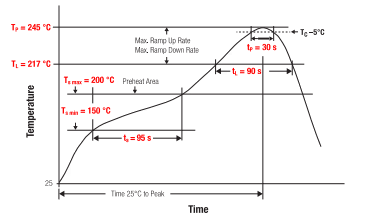
Figure 11: Classification reflow profile for WE THR products
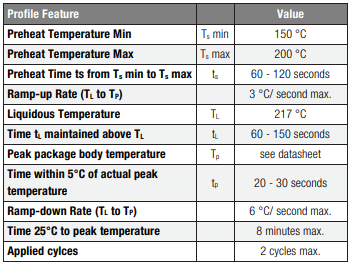
Table 1: Classification reflow profiles
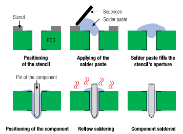
Picture 12: Schematic flow chart of the reflow processInspection
The IPC-A-610 standard can be used to inspect THR components. The tests are based on the acceptance criteria for electrical components for soldering joints of through-hole components. Non-visible areas were checked by means of polished cross section images. The following criteria served as a basis:
- a minimum of 75 % solder coverage on both sides of the leads, see figure 13.
- less than 30 % air cavities, see figure 14.
- 100 % wetting at the surface of the drilling hole and on the component lead
3.7. Result of our part
The pilot lot of our part has been inspected visually per IPC-A-610E. It was passed based on the acceptance criteria for electrical components for soldering joints of through-hole components. See figure 11.
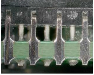
Figure 13: Soldering result (cross section)
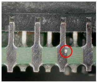
Figure 14: air cavity (cross section)
4 Summary
This application note introduces the critical issues that need to be considered when implementing through hole reflow process. From component selection, PCB design, stencil design and process set. We believe that the through-hole reflow technology is very useful, as it can save time money and manpower. Furthermore, it can be applied for wide applications such as communication, automotive, industry, etc.
A. Appendix
A.1. References
[1] Guillaume Greniner, “THR (Through - Hole Reflow) Technology” eiSos news_THR components.
[2] “Pin in Paste Application Note”, Lifflefuse Inc.
[3] “Basics Connectors for SMT production Through - Hole Reflow” Phoenix Contact GmbH & Co. KG
IMPORTANT NOTICE
The Application Note is based on our knowledge and experience of typical requirements concerning these areas. It serves as general guidance and should not be construed as a commitment for the suitability for customer applications by Würth Elektronik eiSos GmbH & Co. KG. The information in the Application Note is subject to change without notice. This document and parts thereof must not be reproduced or copied without written permission, and contents thereof must not be imparted to a third party nor be used for any unauthorized purpose. Würth Elektronik eiSos GmbH & Co. KG and its subsidiaries and affiliates (WE) are not liable for application assistance of any kind. Customers may use WE’s assistance and product recommendations for their applications and design. The responsibility for the applicability and use of WE Products in a particular customer design is always solely within the authority of the customer. Due to this fact it is up to the customer to evaluate and investigate, where appropriate, and decide whether the device with the specific product characteristics described in the product specification is valid and suitable for the respective customer application or not. The technical specifications are stated in the current data sheet of the products. Therefore the customers shall use the data sheets and are cautioned to verify that data sheets are current. The current data sheets can be downloaded at www.we-online.com. Customers shall strictly observe any product-specific notes, cautions and warnings. WE reserves the right to make corrections, modifications, enhancements, improvements, and other changes to its products and services. WE DOES NOT WARRANT OR REPRESENT THAT ANY LICENSE, EITHER EXPRESS OR IMPLIED, IS GRANTED UNDER ANY PATENT RIGHT, COPYRIGHT, MASK WORK RIGHT, OR OTHER INTELLECTUAL PROPERTY RIGHT RELATING TO ANY COMBINATION, MACHINE, OR PROCESS IN WHICH WE PRODUCTS OR SERVICES ARE USED. INFORMATION PUBLISHED BY WE REGARDING THIRD-PARTY PRODUCTS OR SERVICES DOES NOT CONSTITUTE A LICENSE FROM WE TO USE SUCH PRODUCTS OR SERVICES OR A WARRANTY OR ENDORSEMENT THEREOF. WE products are not authorized for use in safety-critical applications, or where a failure of the product is reasonably expected to cause severe personal injury or death. Moreover, WE products are neither designed nor intended for use in areas such as military, aerospace, aviation, nuclear control, submarine, transportation (automotive control, train control, ship control), transportation signal, disaster prevention, medical, public information network etc. Customers shall inform WE about the intent of such usage before design-in stage. In certain customer applications requiring a very high level of safety and in which the malfunction or failure of an electronic component could endanger human life or health, customers must ensure that they have all necessary expertise in the safety and regulatory ramifications of their applications. Customers acknowledge and agree that they are solely responsible for all legal, regulatory and safety-related requirements concerning their products and any use of WE products in such safetycritical applications, notwithstanding any applications-related information or support that may be provided by WE. CUSTOMERS SHALL INDEMNIFY WE AGAINST ANY DAMAGES ARISING OUT OF THE USE OF WE PRODUCTS IN SUCH SAFETY-CRITICAL APPLICATIONS.
Application Note as PDF: ANP078 WE-RJ45 LAN for Through-Hole Reflow
USEFUL LINKS
Application Notes www.we-online.com/appnotes
REDEXPERT Design Plattform www.we-online.com/redexpert
Toolbox www.we-online.com/toolbox
Produkt Catalog www.we-online.com/products
CONTACT INFORMATION
Tel. +49 7942 945 - 0
Würth Elektronik eiSos GmbH & Co. KG
Max-Eyth-Str. 1 ⋅ 74638 Waldenburg ⋅ Germany
