
Application Note
RF Gain Block Amplifier with Integrated Ferrite Bead for Broadband Operation
ANP101 BY JOANNE WU
1 Introduction
The constantly growing demand for devices with wireless communication ports is pushing devices to operate at increased bandwidths over a wide frequency range. It is becoming increasingly important to ensure every design engineer has an all-purpose radio frequency (RF) amplifier at hand. It is possible to design a versatile RF amplifier that will fit into many categories, for example from 5G systems to radio and antenna equipment applications. The standard process when changing the operating frequency range of an existing RF amplifier usually requires a new design that includes extensive simulation and a new circuit board. However, this may not be necessary, depending whether the new frequency range is far from the original.
There are some key parameters to consider like frequency and gain during design of an amplifier for the high-frequency range. By selecting the optimal passive components, it can extend or improve the transmission characteristics of the amplifier device. Not only with components, but also a well-designed layout that can transmit the high-frequency signal and DC current to supply the amplifier in a single line without disturbances and interferences with each other; improves the efficiency in the high-frequency range.
A key component for this smooth operation of the transmission of mixed signals (RF and DC) lies in the RF bias inductor for decoupling the RF from the DC supply. Apart from the usual practice of using a standard inductor, another suitable alternative is the use of a chip bead ferrite. To compare and evaluate the chip bead ferrite and the inductor in this application, an evaluation board of an RF amplifier is created to verify the outcome with measurements (Figure 1). This application note describes circuit design considerations and compares alternative recommendations to achieve optimum parameters through two RF amplifier examples. The advantage of a quality general purpose RF amplifier is that the user can apply the same design for many different applications, since there is usually neither time nor budget for changes.

Figure 1: RF gain amplifier evaluation board
2 Component Selection
In the following section, passive components to achieve broadband operation are selected and an introduction of two RF gain amplifiers is given. The aim is to provide an alternative method of selecting components compared to the usual recommended configuration circuit found in the data sheet. Online tools such as the REDEXPERT from Würth Elektronik, are a helpful aid to compare electrical characteristics of components using real measured values from the same series type with each other. Therefore, a detailed description on choosing the most suitable inductors and capacitors is explained in this section.
2.1. RF Gain Amplifier
Two similar gain block amplifiers were selected to conduct the measurement. The ADL5544 and the HMC311ST89, both from Analog Devices [1], [2]. Found in the following Table 1, each of their specifications are a near match. Key differences are the specified broadband operation, the noise figure and the bias control circuit, where the ADL5544 device has an integrated internal bias circuit; and, the HMC311ST89 requires an external bias circuit.

Table 1: The selected RF gain amplifiers
2.2. ADL5544 Gain Amplifier
The ADL5544 is a single-ended RF/IF gain block amplifier with a fixed gain of 17 dB and a broadband operation from 30 MHz to 6 GHz. It has an independent bias control circuit integrated as part of the IC. The application information in Figure 2 is taken from the data sheet. The schematic corresponds to the basic circuit of the amplifier, the table shows a list of recommended LC configurations for operation of the device at various frequency bands.
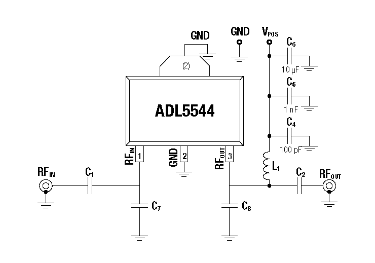

Figure 2: ADL5544 application information diagram and table. Adapted from [1]
As tabulated, the configuration of the board may be adjusted to utilize the best performance of the device according to the frequency bands in application. The recommended AC coupling capacitors (C1 and C2) are between the values 100 nF and 100 pF. As for the RF bias inductor (L1), three separate inductor values are recommended for the respective three frequency ranges. This is standard during the designing stage and gives the user the flexibility to determine the frequency spectrum and change components accordingly.
2.3. HMC311ST89 Gain Amplifier
The HMC311ST89 is a single ended gain block amplifier. Similar to the ADL5544, it is capable of providing up to 16 dB of gain over a frequency range of DC to 6 GHz. However, this IC does not come with an integrated bias control circuit, therefore an external biasing resistor RBIAS is required (Figure 3). For a more stable current control output, a small, low power and low cost linear LED driver can be used. The LED driver BCR402W, for example, offers higher current control at a very low voltage drop in contrast to a bias resistor [3].


Figure 3: HMC3311ST89 application information diagram and table. Adapted from [2]
The AC coupling capacitors (C1 and C2) are all valued at 100 pF, except in the frequency range around 50 MHz, where the target value, according to the table in the data sheet, is 0.01 μF. In contrast, a range of different RF bias inductors (L1) is recommended depending on a specific frequency. The next section of this article explains the selection of RF components to yield a broadband application.
2.4. RF Bias Inductor Selection
As the two RF amplifiers have similar properties, the RF bias inductor is chosen accordingly to perform in the broadest frequency spectrum possible in both circuits. The RF bias inductor, also known as RF choke, is a component used to decouple high frequency signals through high impedance while passing DC. Thus, inductor selection is dependent on the operating frequency range of the selected amplifier. This means that different value inductors are dedicated to perform at its best in a specific frequency range. The disadvantage is when design specifications change and a new inductor needs to be selected. Here the ferrite bead is introduced as an unconventional alternative in choosing a RF bias inductor solution that allows universal use at a lower cost.
Table 2 shows a list of selected multilayer ferrites and inductors that have been compared for use as RF chokes in the application described. First, the WE-KI and the WE-KI HC (high current) are wire wound ceramic inductors ideally for RF applications. The recommended values from the manufacturer’s data sheet (Figure 2 and 3) are 56 nH and 100 nH. These inductors will become the bases of the comparison to the alternative chip bead ferrites.

Table 2: The selected inductor values
Ferrite beads are passive components with a high attenuation over a broad frequency range. Their function is mainly to eliminate RF noise in transmission lines, acting as an impedance (frequency dependant resistor), which allows DC signals to pass through and “filter out” AC signals. As ferrite beads are typically given in impedance values, we need to calculate inductance to correlate to the recommended application. The inductance of a ferrite bead can be estimated from the impedance at a specific frequency. This approximated inductance L is calculated using Equation (1), where Z is the impedance of the ferrite bead at the specified frequency, and f is the specified frequency.
 (1)
(1)
For inductors, factors like DC bias current have less impact on the preservation of inductance until the inductors are used beyond the saturation current. In contrast, DC bias has a prominent influence on ferrite beads and the current flowing through the component changes the inductance over a specific frequency range. Ferrite beads saturate as a function of the flowing bias current, changing the impedance curve in the lower frequency (<100 MHz) at the same time, shifting the self resonant frequency (SRF) higher in frequency. Therefore, an approximation of the bias current should be taken into consideration in order to approximate the correct inductance under application. Würth Elektronik’s measurement based online design platform REDEXPERT, can be used to determine the impedance and other electrical characteristics of any chip bead ferrite at any operating frequency and DC bias current. Taken from the data sheet the power consumption of the amplifier is about 55 mA. As shown in Figure 4, the smallest rated current value provided for all selected ferrite beads in REDEXPERT is 100 mA. This current is a factor of 2 higher than the one used in the application, so that the curve shown leads to a lower impedance and thus represents a less favorable case (~worst case).
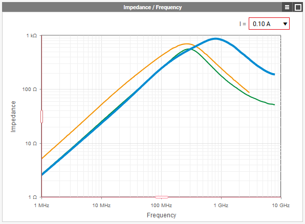
Figure 4: Impedance curve comparison of WE-CBF 742792656 (yellow), WE-CBF HF 742863160 (blue) and WE-TMSB 74269262601 (green)
at 0.1 A
The ferrite bead WE-CBF HF 742863160 with a bias current of 100 mA clarifies the situation as an example. The inductance value L that results from the impedance Z = 240 Ω at a frequency f = 100 MHz is L = 382 nH. The inductances calculated for different frequencies are listed in Table 3, showing from 100 to 500 MHz range the inductance is from 382 to 239 nH respectively. Although this inductance range is lower than the recommended range, it can be compensated by adding a second chip bead in series to sum up the total inductances. Doubling the inductance will extend the range from 764 to 478 nH. This becomes an acceptable range especially since the impedance in the example shown here is lower because a higher bias current test condition (TC) has been used.

Table 3: Calculated inductance of WE-CBF HF 742863160
At the high frequency end, the single WE-CBF HF can achieve an inductance of 5.3 nH, well within range of the recommended 12 nH. By placing two ferrites in series it is possible to cover the full usable spectrum of the gain block amplifier. Overall ferrite beads have the possibility to provide the widest range of frequency going through, giving the broadest frequency spectrum. As opposed to individually selected inductors that are only suited for different frequency ranges. Although in standard applications ferrite beads and ceramic inductors have different applications, here it is a suitable substitution and may perform better than a standard inductor.
2.5. DC Block Capacitor Selection
The RF path requires a DC blocking capacitor. DC blocks stop the flow of DC while allowing the higher frequency RF signals to pass through. They can be thought of as a high pass filter and are usually designed in by placing capacitors in series with the RF transmission line. However adding a DC blocking capacitor will introduce a discontinuity in the transmission line at high frequencies and therefore choosing a suitable capacitor is key.
The smaller value capacitors normally have higher self-resonant frequencies (SRFs), while the larger values have lower SRFs. This can be evaluated using the REDEXPERT graph as depicted in Figure 5. Here are shown the impedance curves of four common capacitor values in different sizes. Both amplifier data sheets recommend using capacitors in 0402 case size valued at 100 pF (light blue curve) and 100 nF (green curve). To achieve optimal results, depending on the frequency range of the application, the capacitor values are chosen to provide a low-impedance path for the signal while able to block DC.
Real capacitors have limited usable frequency ranges due to their SRF. Judging from the impedance graph, capacitors with larger capacitance values, compared to capacitors with lower capacitance values, have a lower impedance SRF point, which is in a lower frequency range. For example, the 100 pF capacitor in size 0402, the SRF point starts at 1 GHz with a high impedance value of 800 mΩ. On the other hand, a 100 μF size 1206 capacitor has a SRF at 1 MHz with an impedance of 2.5 mΩ. This means that the recommended capacitor (100 pF, 0402) has ten times more impedance to begin with than the 100 μF in 1206 size.

Figure 5: Selection of capacitors WCAP-CSGP 1206 100 μF (dark blue), 0805 47 μF (yellow), 0402 100 nF (green) and 0402 100 pF (light blue) (link)
Apart from having low impedance, it also requires broadband usability to realize the full spectrum of the amplifier. Summarized in Table 4 is a breakdown of the impedance values from 10 kHz to 1 GHz.

Table 4: WCAP-CSGP capacitors, impedance in different frequency ranges
3 PCB Layout Design
RF layout techniques should be used to maximize performance of the gain block amplifier. It is important to minimize impedance mismatch loss which causes disruptions when signal passes from one impedance not aligned to another impedance. Therefore, it is ideal that the signal line tracks are designed with grounded coplanar waveguides that should have 50 Ω impedance in order to prevent reflections. Here the standard 2-layer PCB setup was used with a TG135 FR4 core material, and a thickness of 1.55 mm. This fixes two of the adjustable parameters, the dielectric constant εr and the thickness used to calculate the waveguide impedance, as shown in Figure 6. Adjusting the width of the trace W and gap G will lower and rise the overall impedance of the line respectively.
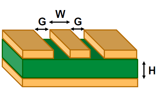
Figure 6: Grounded coplanar waveguide
Furthermore, good ground techniques should be applied to establish a low impedance connection to the ground plane. Adequate number of via holes, shown in Figure 7, should be used to connect the top and bottom ground planes, creating a via fence. Having the via fence helps to capture stray fields between ground to reduce coupling and minimize losses. This is particularly important along both sides of the coplanar waveguide, but also can be seen around components and on the edges of the circuit board to reduce uncontrolled coupling (see Figure 8).

Figure 7: Cross-sectional view of a grounded coplanar waveguide with via fence on both sides

Figure 8: PCB layout top layer utilizing the via fence
Most ICs require a solid ground plane directly underneath the component to ensure good grounding. Known as a ground paddle, the use of multiple thermal vias connecting the top side with the bottom side is to further achieve a distributed heat transfer by providing good heat sink capability in several layers. The following example in Figure 9 is a recommended configuration that shows three via holes embedded inside the land pattern and with an additional via fence surrounding the chip. This supports the amplifying chip with a stable ground connection.

Figure 9: Vias embedded in the ground plane of land pattern
Solder resist (or solder mask) is a thin layer of coloured material printed on top of the copper trace layer. This protection layer prevents against oxidation and offers electrical insulation to protect areas from taking solder. This provides many advantages; for example, to have solder only where it is needed, or to reduce short circuits caused by solder bridges from traces that are closely next to each other. In contrast, the solder resist has a negative influence on RF transmission lines due to its lossy properties. Solder resist has a high dielectric constant and therefore adds to the dielectric constant of the system. As it is applied as a liquid, the thickness may not be well controlled and is unpredictable; this means, the characteristic impedance will become harder to control. Simulation models also often do not take into account the resist thickness and even if they do, the impact cannot be modelled accurately. At high frequency, having no solder resist will reduce the loss and achieve better RF transmission. Figure 10 shows the layout with partial cutout of the solder resist (yellow areas).

Figure 10: Removal of solder resist layer (yellow)
It is important to also include solder pads in the ground plane for the SMA connector. Not only does this mechanically strengthen the connector to the PCB, it also reduces drawbacks due to the gap between connector housing and PCB. Having a gap (space) between the connector and the PCB can cause unwanted matching problems, hence a solder connection on the bottom side gives the connector an additional stable ground connection.
It is not easy to find a suitable capacitor value for the DC block capacitor and to choose a suitable size. The 1206 size of the DC block capacitors is considered large in this application, as it is nearly equal in width to the signal trace. In order to compensate the additional stray capacitance on the trace due to the dimensions of the capacitor, not just the width but also the extra height of the component, must be balanced by adjusting the gap track width across the capacitor. The stray capacitance can be compensated by increasing the gap between the trace and the ground shield as shown in Figure 11.

Figure 11: Compensating for the capacitor by increasing gap trace width
Changing the RF trace width causes discontinuities, which varies the impedance along the RF path. This is not desired as it causes reflections and field conversions, therefore it is best to keep it consistent. To measure the impedance of the signal line, a time domain reflectometry (TDR) measurement can test the trace for impedance jumps (discontinuities). Similarly, the reflection and transmission measurements from S-parameters can further provide information about the performance of the board and can be used to analyse whether board loss has an impact on the application. The following Figure 12 shows a good example of the reflection of a RF signal line on an optimized PCB board.

Figure 12: Reflection behavior of an RF transmission line (S11)
4 Measurement Setup
The aim of the measurement is to evaluate the transmission characteristics of RF signal over the frequency range. First, to define the measurement setup in order to understand the results. The transmission characteristics of the testboard is shown in Figure 13 and Figure 14, where S11 is the reflection at RF-In and S21 is the attenuation between RF-In and RF-Out. DC is supplied externally through DC-In in which gets combined with RF-Out.

Figure 13: Evaluation board with DC-bias only and no RF gain amplifier
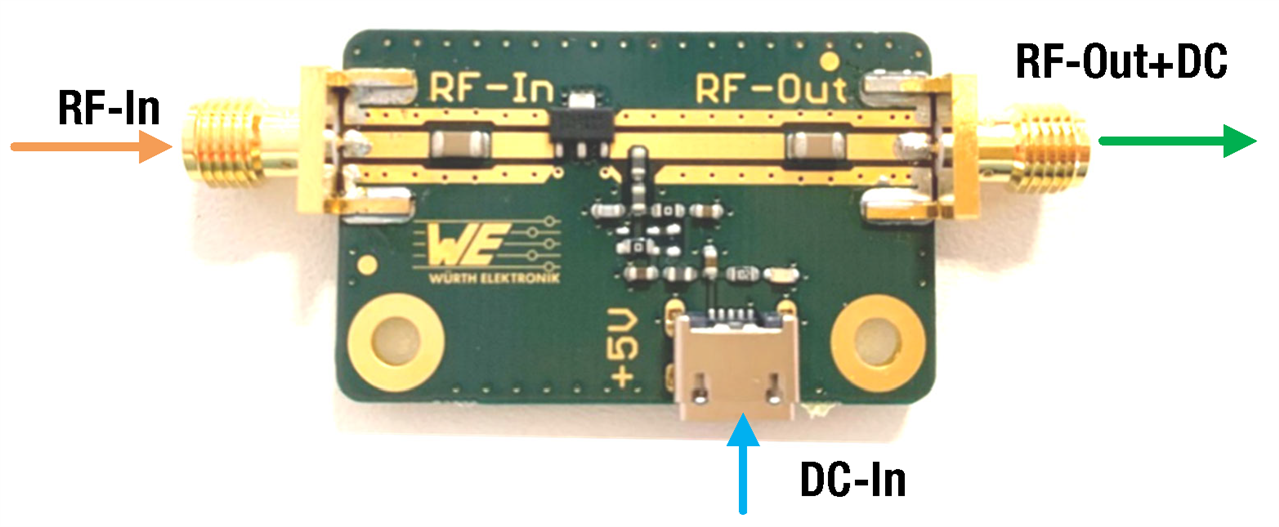
Figure 14: Evaluation board with RF gain amplifier
5 Evaluation
The aim of the measurement is to compare the results of traditional standard approach verses an unconventional approach of designing a RF gain amplifier. In order to understand what differences will affect the performance of the RF gain amplifier, the RF-bias inductor component is changed. We will draw our conclusions based on how broadband the RF gain amplifier can be used.
First, the behavior of the evaluation board without amplifier, as shown in Figure 13, is analyzed. This will assess the characteristic of the RF and the DC system before including the RF gain amplifier. The standard recommended approach of RF inductors is compared with the ferrite bead. This is followed by a comparison of different ferrite bead series, which include the WE-CBF, WE-CBF HF and the WE-TMSB. Finally, to evaluate the behavior of the RF gain amplifier implemented into the overall RF and DC system.
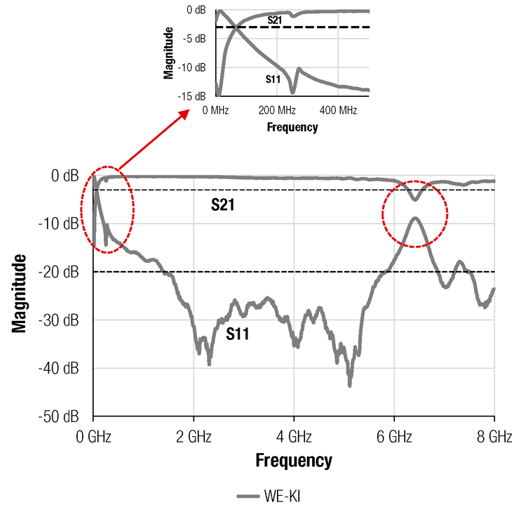
Figure 15: Transmission of RF signal with WE-KI 744761156A
Figure 15 shows the S-parameter S11 and S21 of a WE-KI 744761156A wire wound ceramic inductor valued at 56 nH used as a decoupling inductor. We can see on the curve S21 that the signal passes through with minimal damping from around 400 MHz to 6 GHz, before reaching an attenuation of 3 dB at about 6.5 GHz. Successful transmission is generally defined between 0 to -3 dB. As an attenuation of 3 dB already corresponds to a transmission ratio of 50 %, i.e. half the power is attenuated, avoid going lower to ensure an effective signal throughput. The attenuation of 3 dB value is indicated by a black dashed line in the below graphs. Below 400 MHz and above 6 GHz, the attenuation increases sharply meaning that in these frequency ranges the signal is hardly amplified any more, which is highlighted in the red dashed circles in Figure 15. In addition, a couple of resonant peaks are present, disrupting the signal transmission and may cause disturbances. An attenuation value of 1 dB occurs at 6 GHz, indicating that 80 % of the signal is transmitted before the attenuation starts to roll off as the frequency increases.
Similarly, correlating to the S11 reflection parameter, the best performing range is between 1.6 GHz to 5.6 GHz. In this region, the reflection is below -20 dB. Depending on the application, the goal of the reflection should be as low as possible which indicates that there are no signals reflected backwards. A reflection of -20 dB corresponds 1 % of the signal reflected. For the purpose of analyzing this application, a threshold value, indicated by a black dashed line, is set at -20 dB in order to achieve good results. Again, the resonances can be seen present at the same frequencies, at 260 MHz and at 6400 MHz. At these two frequencies, discontinuities can be assumed because of the low S11 value. These discontinuities cause signal losses. Many factors can cause discontinuities and resonance peaks in this application. For example, the RF inductor resonating with the filter capacitors or self-resonation of the inductors due to its high Q factor. Since generally inductors have high Q factors, they are more prone to unwanted resonations.
With the use of a traditional RF inductor, a broadband operation of this evaluation board can already be achieved. A well designed PCB with RF layout designs in consideration has proven to produce better performance at higher frequencies and broaden the overall frequency spectrum. An unconventional design that can further improve the broadband operation is to use a ferrite bead.
Next, with the same design but instead of a RF inductor, a ferrite bead 742863160 from the WE-CBF HF series is used.
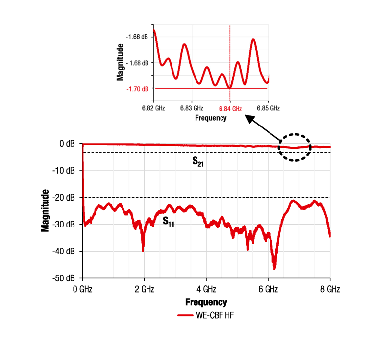
Figure 16: Transmission of RF signal with WE-CBF HF 742863160
The S-parameter shown in Figure 16 indicate that the throughput S21 stays above -3 dB in the range from 0 Hz to 8 GHz without resonance interruptions. The lowest transmission is -1.70 dB at 6.84 GHz, corresponding to a transmission ratio of 68 %. A very broad spectrum was achieved from 30 MHz to 8 GHz in this application. Similarly the results are reflected when analyzing the reflection loss S11. Throughout the whole measured frequency spectrum, the reflection stayed below -20 dB, achieving a reflection smaller than 1 %.

Figure 17: Comparison of RF signal WE-KI inductor with WE-CBF HF ferrite bead
Figure 17 shows the comparison between the previously analyzed WE-KI (grey lines) with the WE-CBF HF (red lines) of the corresponding S-parameters S11 and S21. Through the comparison graph, it can be clearly seen the main advantages of using a ferrite bead over a RF inductor. In the lower frequency range, the signals are not affected by resonance peaks. Inductors generally have a much higher Q-factor than ferrite beads. Consequently, the higher the Q-factor, the greater the amplitude of the resonance peaks are formed. These peaks are furthermore reflected in the reflection loss S11 of the RF inductor. In comparison, the ferrite bead has a much more stable performance over the whole spectrum, with the reflection sitting below -20 dB throughout.
Overall, the measurement confirms that by using ferrite beads better transmission is achieved over the entire frequency range. Not only has it broadened the useable frequency range, the clarity of the transmission signal is also more stable. However ferrite beads also have disadvantages from its characteristics behavior. High frequency chip bead ferrites generally have lower rated current values due to its high impedance. Therefore using ferrite beads in place of RF inductors may only be suitable for low current applications.
5.1. With DC-bias

Figure 18: Transmission of RF signal WE-KI (grey) and WE-CBF HF (red) under current bias of 0.1 A
Applying DC-bias changes the overall system and it can be seen that the transmission characteristics over frequency is smoother. The current reduces the inductance and impedance values and can also shift the resonance frequency of components. This effect can be seen in Figure 18, where the application is under DC current bias of 0.1 A. The grey curve shows the measurement results of WE-KI inductor and the red curve shows the results of WE-CBF HF both with DC-bias. Usually a ferrite bead’s point of SRF shifts to a higher frequency with increasing current while the impedance decreases. For a capacitor, the SRF shifts to a higher frequency with increasing voltage while the impedance increases. On the other hand, RF inductors are generally more stable in saturation than ferrite beads. This measurement with DC-bias does not affect the overall performance when taking into consideration designing in the correct components.
To compensate for the lowered impedance (and inductance) values of the ferrite bead and capacitors must be selected under the right bias conditions. This can be designed with the help of Würth Elektronik’s online tool REDEXPERT. For inductor and capacitor selection please refer to Section 2.2 and Section 2.3 respectively.
5.2. Comparison of different Ferrite Beads

Figure 19: Transmission of RF signal with WE-CBF HF, WE-CBF and WE-TMSB
Previous comparison was made with a RF inductor and a ferrite bead. However there are also different characteristics of a ferrite bead which show different results in the transmission characteristics of the application described here. This comparison shown in Figure 19 looks at three multilayer ferrite series WE-CBF, WE-CBF HF and WE-TMSB from Würth Elektronik. Although they are all ferrite beads with similar electrical properties (impedance verses frequency comparison shown in Figure 4), their effects in terms of transmission characteristics in this application differ.
The S-parameter values for the WE-CBF and the WE-TMSB are similar. In the reflection S11, they stay below the -20 dB threshold value until 1.6 GHz before ascending above the limit until the end of the measured frequency range. Discontinuities and resonances appear in this region and can be seen reflected in the S21 throughput attenuation as well. The attenuation of 3 dB at 4.8 GHz and 4.1 GHz causes 50 % of the signal to be lost.
Overall the WE-CBF HF outperformed the other two series. One reason for the difference is due to the internal structure of the multilayer ferrite bead. For example the construction of the internal windings of the WE-CBF are layered horizontal, while for the WE-CBF HF the windings are layered vertically. Other factors may be due to specific electrical properties like saturation rating. For further detailed information regarding the differences, refer to application note ANP045.
The comparison shows that when selecting components, it is important not only to choose alternative components, but also the right ones for the application. Lastly the results of both the design of the PCB and passive components selected with an operating gain amplifier example are evaluated.
5.3. Comparison in the application with RF Gain Amplifier
The two RF gain amplifiers ADL5544 with integrated bias and HMC311ST89 without integrated bias were introduced in Section 2.1. First to evaluate the results between a RF inductor and a ferrite bead. Based on the data sheet, both RF gain amplifiers are capable to be used up to 6 GHz.

Figure 20: S-parameter of ADL5544 RF gain amplifier comparing WE-KI and WE-CBF HF
Figure 20 shows the transmission characteristics for the ADL5544 amplifier with a WE-KI RF inductor. The output gain starts at 17.9 dB and decreases contiuously to 10.67 dB at 8 GHz. As for the WE-CBF HF ferrite bead, the output gain is around the same and decreases to 10.16 dB respectively. This indicates that both components have a similar gain output profile.
In this application, the current bias is seen as a high impedance element to the RF signal. The current source should enable the signal to remain as unaffected as possible and also provide a direct current for the supply of the amplifier module. However, a RF inductor does not provide continuous high impedance over a wide frequency range, but usually only over an intrinsically limited range, e.g. 200 MHz to 2 GHz. In addition, the impedance curve has a sharp self-resonance peak, which is due to the parasitic capacitance. That is why there are clearly noticeable peaks present in the RF inductor application. As can be seen in Figure 20, these are at 1572 MHz and 7050 MHz in the case of the throughput attenuation S21. At these frequencies, significant discontinuities are also evident, as shown by the reflection loss S11.

Figure 21: S-parameter of HMC311ST89 RF gain amplifier comparing WE-KI and WE-CBF HF
In comparison between the throughput attenuation S21 in Figure 20 and Figure 21, HMC311ST89 gain amplifier achieved a smaller gradient than the ADL5544, keeping the gain throughout the frequency spectrum stable. One factor to consider is the influence of the bias network. The ADL5544 has an integrated bias, while the HMC did not.
This allowed the flexibility to design a good external bias circuit to support the RF and DC signals.The overall comparison between a RF inductor (WE-KI) and ferrite bead (WE-CBF HF) shows that the performance of the ferrite bead can achieve a more stable performance without resonances.
6 Conclusion
Broadband amplifiers are often needed in receiving applications when using antennas, to reproduce a wide range of small signals with low noise. The results show that under practical conditions with DC bias effects, the RF circuit design is crucial for overall performance. The supply voltage for many amplifier modules cannot be applied directly, but must be coupled in via the signal line. Therefore, a high impedance component over the broadest possible frequency range is used to ensure the complete RF signal can be amplified by the module and is not affected or attenuated by the DC bias circuit. In this application an alternate component, a ferrite bead was investigated compared to the traditional method, a RF inductor. With the ferrite bead a broader frequency spectrum and higher stability due to lower reflections, i.e. better matching, could be achieved. The ferrite WE-CBF HF had a high and stable impedance and therefore a high decoupling with low peak resonances while the standard choke WE-KI had a lower bandwidth and visible resonances throughout. On the other hand, comparing the two RF gain amplifiers, HMC311ST89 with external bias was better than the ADL5544 with integrated bias. The goal to achieve a broader usable frequency spectrum application has been achieved.
A. Appendix
A.1. Schematics


A.2. Bill of Materials
| Index | Description | Size | Value | Order Code |
| C2, C9 | WCAP-CSGP | 1206 | 100 uF, 6.3 V, X5R Class II | 885012108005 |
| L3 | WE-KI | 0603 | 56 nH, 40, 0.31 Ω | 744761156A |
| L3, L4 | WE-KI HC | 0603 | 100 nH, 35, 0.54 Ω | 744917210 |
| L3, L4 | WE-CBF | 0603 | 750 Ω, 900 mA, 0.35 Ω | 742792656 |
| L3, L4, L5 | WE-CBF HC | 0603 | 600 Ω, 500 mA, 0.9 Ω | 742861160 |
| L3, L4 | WE-TMSB | 0603 | 600 Ω, 1500 mA, 0.1 Ω | 74269262601 |
| IC1 | 30 MHz to 6 GHz RF/IF Gain Block | - | - | ADL5544ARKZ-R7 |
| IC1 | InGaP HBT Gain Block | - | - | HMC311ST89 |
| IC2 | Linear LED Driver IC | - | 18 V, 20 mA | BCR402W |
| LED1 | WL-SMCD | 0603 | 60 mcd, 2.0 V, 140° | 150060VS55040 |
| J2 | Micro USB 2.0 Type B | - | SMT Horizonal | 629105150521 |
| CON5, CON6 | SMA PCB End Launch Jack Flat Tab WR-SMA | - | 1.1 mm Thickness | 60312202114512 |
A.3. References
[1] A. Devices, "30 MHz to 6 GHz RF/IF Gain Block,” ADL5544 Data sheet, Rev. A.
[Online] Available: https://www.analog.com/media/en/technical-documentation/data-sheets/ADL5544.PDF [Accessed: Dec. 03, 2021].
[2] A. Devices, "InGaP HBT GAIN BLOCKMMIC AMPLIFIER, DC - 6 GHz,” HMC311ST89/311ST89E Data sheet, v04.0517.
[Online] Available: https://www.analog.com/media/en/technical-documentation/data-sheets/hmc311st89.pdf [Accessed: Dec 03, 2021].
[3] I. Technologies, "LED Driver BCR402W," Rev. 2.0.
[Online] Available: https://www.infineon.com/dgdl/Infineon-BCR402W-DataSheet-v02_00en.pdf?fileId=db3a30431400ef68011407c5054c0192 [Accessed: Dec. 03, 2021].
DIRECT LINK
ANP101: RF Gain Block Amplifier with integrated Multilayer Ferrite for Broadband Operation
USEFUL LINKS:
Application Notes : https://we-online.com/en/support/knowledge/application-notes
Services: https://we-online.com/en/products/components/service
Contact : https://we-online.com/en/support/contact
CONTACT INFORMATION
Würth Elektronik eiSos GmbH & Co. KG
Max-Eyth-Str. 1, 74638 Waldenburg, Germany
Tel.: +49 (0) 7942 / 945 – 0
Email: appnotes@we-online.de

