Gigabit Power over Ethernet Interface from an EMC perspective
ANP122 BY Adrian Stirn
01. INTRODUCTION
The “GB PoE+ -Ethernet-USB” adapter was developed on the basis of the reference design “GB-Ethernet-USB Adapter”, which operates without Power over Ethernet (PoE).
The “GB PoE+ - Ethernet-USB” adapter has three interfaces:
- a USB Type-C
(USB 3.1)
- a RJ45/Ethernet 1 Gigabit interface with integrated Power-over-Ethernet (PoE+) supply
- a terminal to the DC-DC converter, with an adjustable output voltage of 6 – 18 V and a maximum output power of 25 W
The board was developed to familiarize the user with PoE technology. As with the design without PoE, the bit error rate and transmission speed can be investigated using a Windows application.
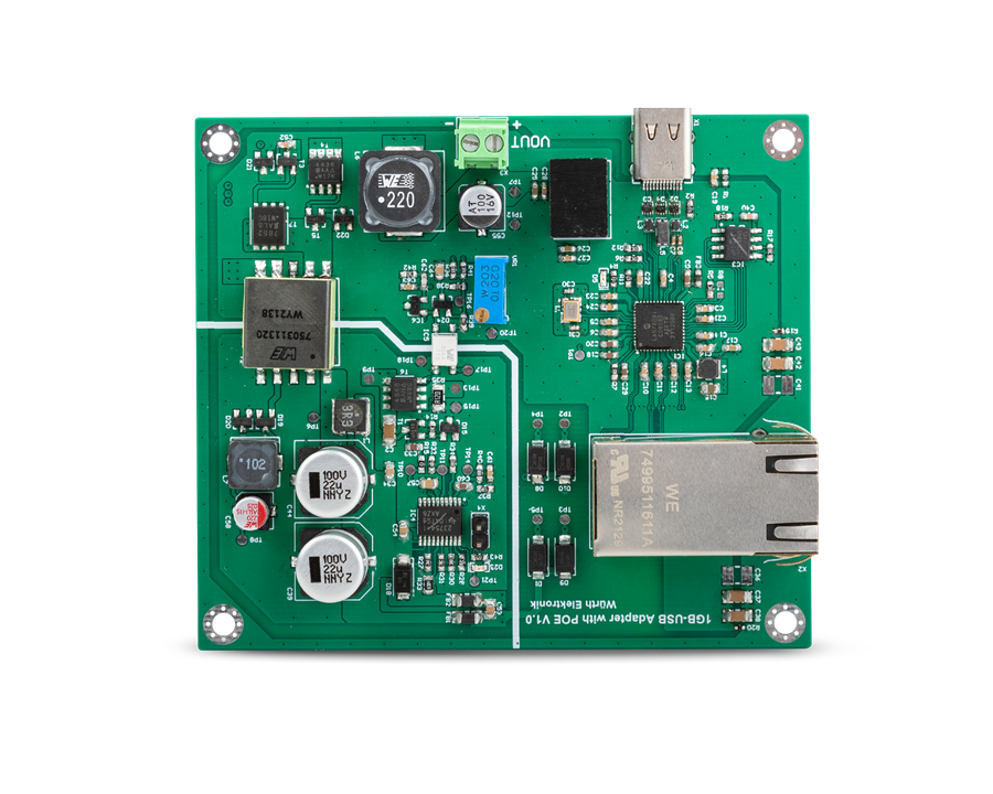
Figure 1: Photo of the test board
The EMC evaluation of the PoE reference design was performed in two steps: First, the board was tested with the power supply shown in Figure 2 without additional filters. Optimizations became necessary during testing, which are described in chapters 3.4 and 3.5, and are included in the optimized circuit diagram in Figure 3. Reference design Note RD022 describes the optimized design in detail.
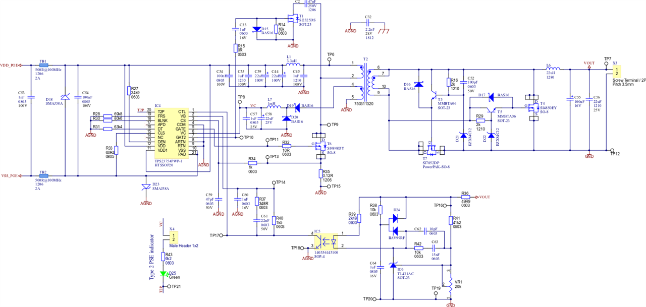
Figure 2: Circuit diagram RD022 Power supply prior to EMC optimization
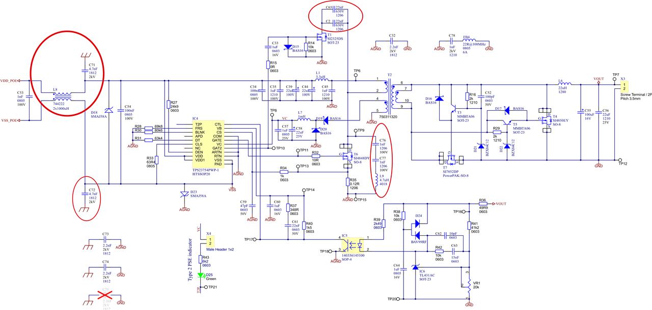
Figure 3: Optimized circuit diagram for RD022 power supply
02. EMC BEHAVIOR OF THE GIGABIT ETHERNET INTERFACE
The EMC behavior of the Gigabit Ethernet interface was already discussed in detail in Reference Design Note RD016 and App Note ANP116. The insights gained there regarding shield connection, cable shielding and the performance of the Ethernet front end, also apply for this App Note. The Gigabit Ethernet design was only extended with the PoE components, the signal section was derived from the Gigabit Ethernet design.
The ideal shield connection determined in ANP116 with two 10 nF capacitors and a parallel SMD varistor is also used in this App Note. The advantages of this Ethernet shield connection have already been sufficiently demonstrated.
03. BASIC EMC APPROACHES FOR THE POE APPLICATION
PoE applications are usually compact electronic devices whose power supply is combined with data communication via an Ethernet interface. So they are usually multimedia devices, which are covered in EMC standardization by CISPR 32 (emission) and CISPR 35 (immunity). The devices tend to be compact and also have short lines apart from the Ethernet cable. Typical devices include:
- WiFi access points
- DECT (Digital Enhanced Cordless Telecommunications) stations
- IP phone
- Surveillance cameras
- Monitoring of indoor climate in storage and production facilities
Applications may be smaller or larger, as shown in Figure 4.
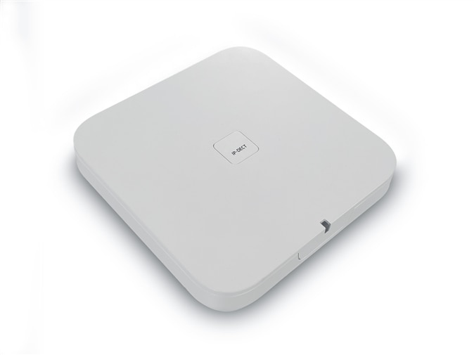
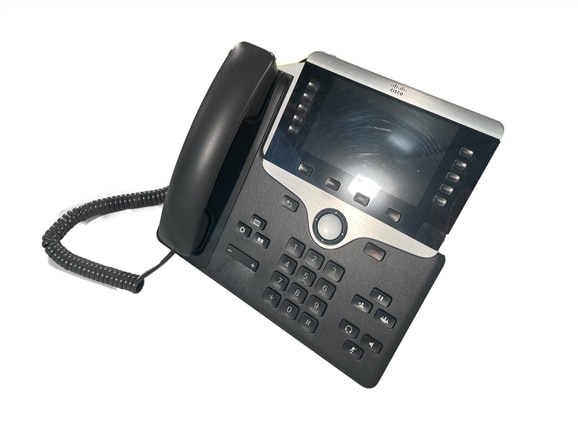
Figure 4: Left: a DECT station as an example of a compact PoE device; right: an IP phone as an example of a larger PoE device
The IP phone is an example of a PoE device with comparatively large dimensions, as the phone receiver cable together with the PCB in the phone is a relatively large structure which can act as an antenna. The two application examples in Figure 4 lead to two possible approaches for the reference design during EMC testing:
- A short output line or compact load resistor (point of load) – compact application.
- Long output lines at the load output – corresponds to a larger PoE application.
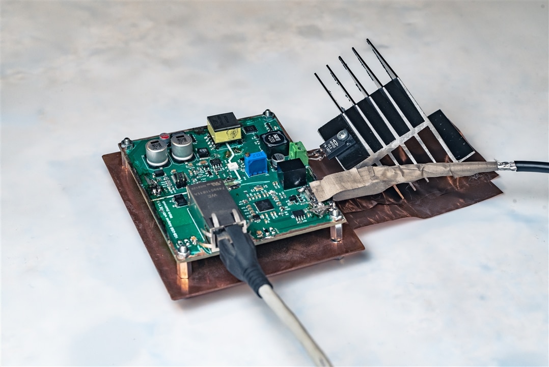
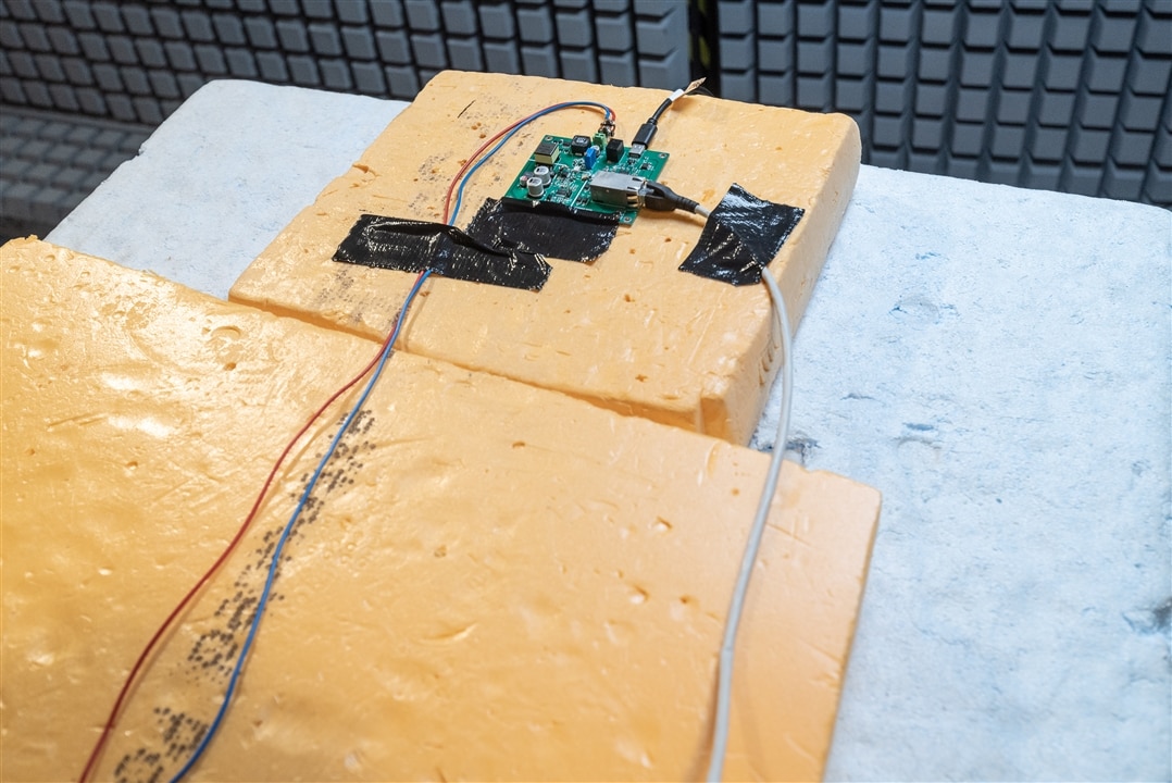
Figure 5: Left: simulation of a compact application (TO-220 load resistor with heat sink); right: simulation of a large application
Figure 5 shows the possibilities of simulating the different applications during EMC testing using the reference design. The advantage of using long cables and a slide resistor during EMC testing is that the load on the switching regulator can be readjusted to always achieve the maximum power. When using the TO-220 compact resistor, the load is fixed at 10 Ω.
3.1 Overview of the EMC test setup and operating parameters
The schematic test setup shown in Figure 6 is similar to the test setup used for testing the Gigabit Ethernet interface and was only extended to include the PoE switch and the load. The focus during EMC testing is on the Ethernet interface, the PoE reference design board, and the various load configurations.

Figure 6: Test setup of the Gigabit PoE board during EMC testing
The USB interface is considered as a short line, the focus during testing is on the Ethernet front end. As the USB interface is needed to operate the board, it is also evaluated in many tests. During the immunity tests, it was found that a direct connection between the USB cable shield and the board GND plane is required for operation at high immunity levels. Only a direct shield connection ensures that the interface remains in a stable operating mode even at high test levels such as 20 V/m above 1 GHz. The load lines are measured with a 2 to 3 m cable length for radiated emission and immunity and should be as short as possible (cable length below 3 m) with regard to EMC. Burst or conducted RF coupling is not applied to the voltage output of the board.
The notebooks required to operate the board and the PoE switch are operated inside a shielded box in order to eliminate their influence on the results of EMC testing as far as possible.
3.2 Influence of the output voltage on emission
Figure 7 shows that the emission of the board is higher at 12 V and 2 A output current than at 18 V and 1.3 A output current. For this reason, some approaches, such as filter design, are carried out at 12 V rather than 18 V.
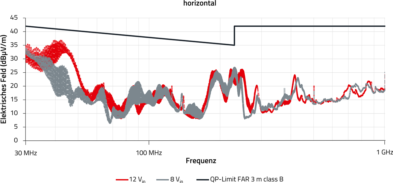
Figure 7: Radiated emission from the Gigabit PoE design when operating with long load lines without an external filter and with shielded cat5e SF/UTP Ethernet cables
3.3 Output filter for long lines and the influence of different load resistances
The circuit diagrams from Figure 2 and Figure 3 show that the isolated switching regulator on the board has no output filter. When connecting long lines and a load resistor, interference may be radiated directly from the switching regulator output, so an output filter may be necessary for large designs or for designs with cables.
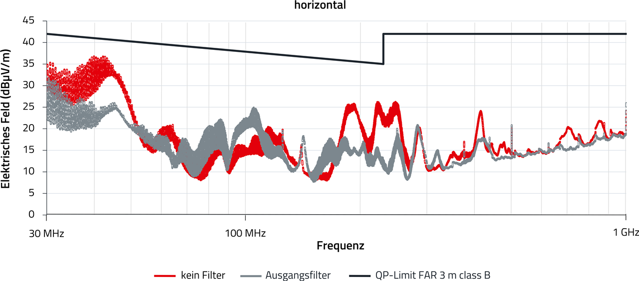
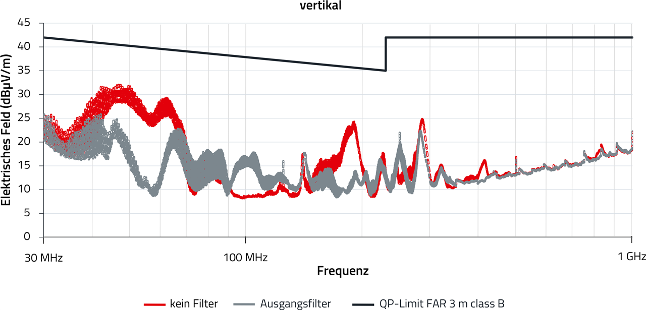
Figure 8: Radiated emission of the Gigabit PoE design operating with long load lines, with shielded cat5e SF/UTP Ethernet cables and an output voltage of 12 V with 2 A load current
The filter from Figure 9 can be used to reduce the radiated interference as shown in Figure 8. This results in an increased margin to the Class B limit of CISPR 32. For larger devices, an output filter is recommended, for which the following components can be used:
- 742792515 – Ferrite Bead (1812 package) with 780 Ohm at 100 MHz.
- 885012209048 – MLCC 4.7 µF X5R 50 V.
- 744237152 – Common-mode choke for signal lines with 17 µH.
The capacitors around the common-mode choke form a differential filter with the chokes leakage inductance. At the same time, any couplings caused by stray magnetic fields from the board into the filters, which would result in a differential current, are short-circuited.
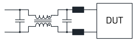
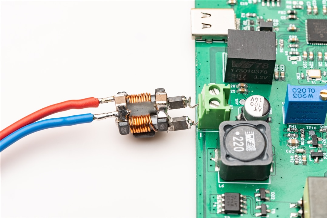
Figure 9: Circuit diagram and photo of the output filter for long load lines
If a load resistor with short leads or a TO-220 resistor is used instead of long lines with a filter (see Figure 10), the emission changes.
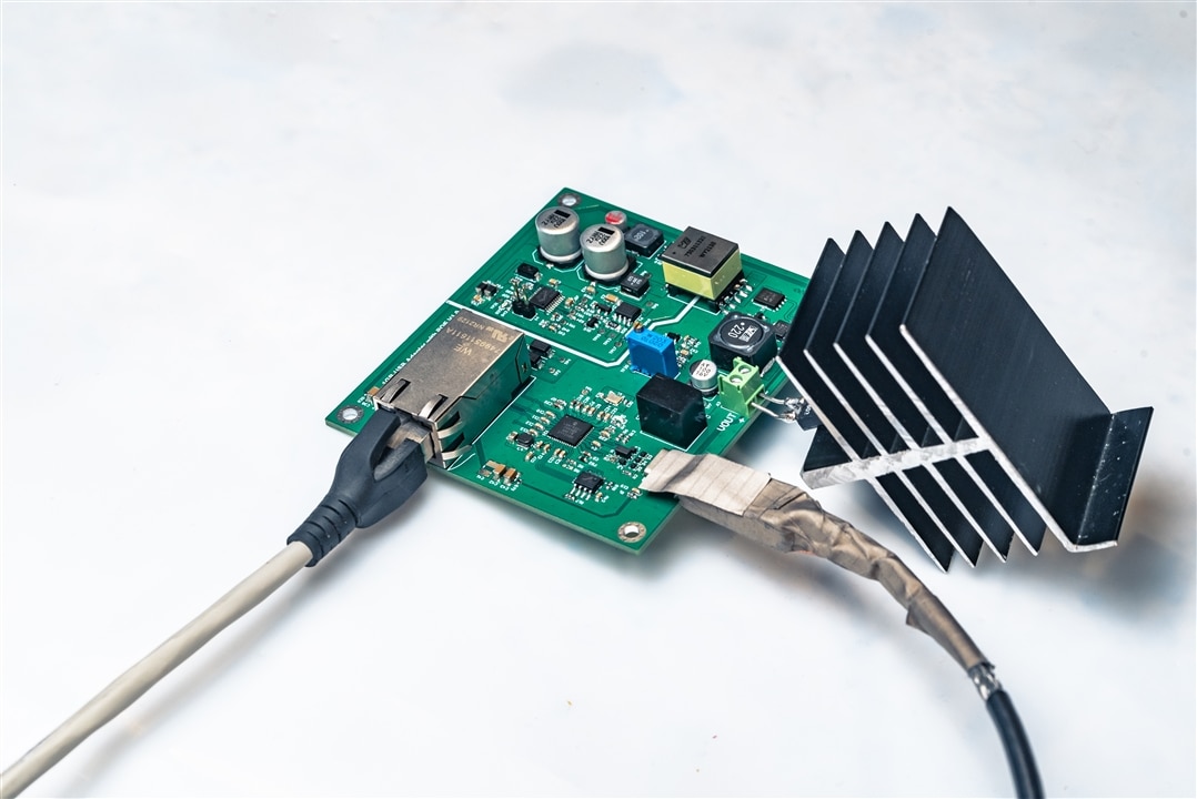
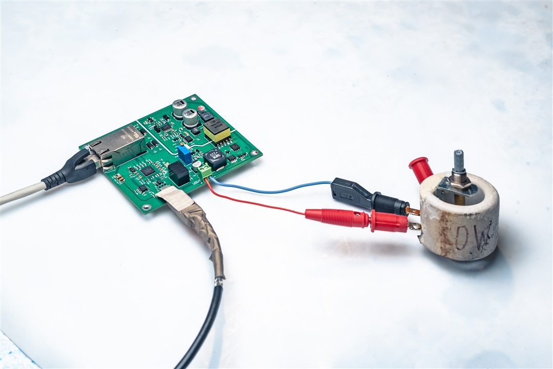
Figure 10: Left: radiated emission with 10 Ω TO-220 resistor and right: load potentiometer with short leads. Without an output filter in each case
Reducing the package size of the load resistors does not improve the emission in the absence of an output filter. Figure 11 shows that the emission with filtered long load lines is partly lower than with compact load resistors.
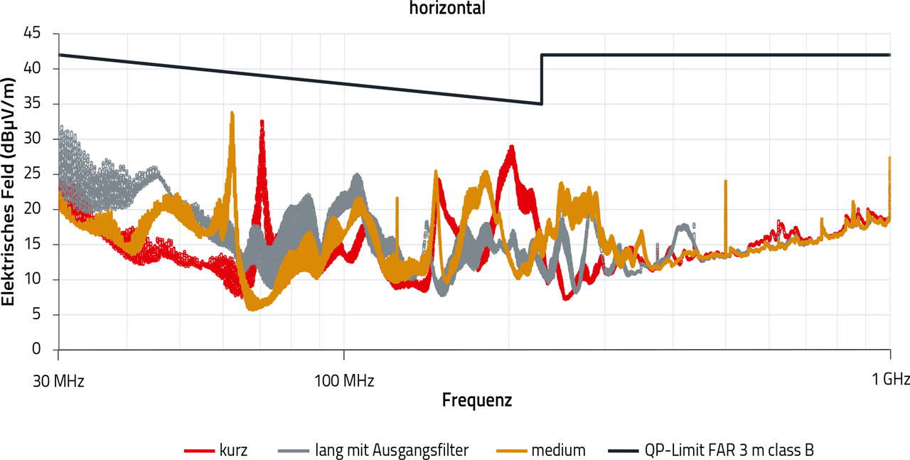
Figure 11: Comparison of emission with different loads at 12 V and 2 A load current with shielded Ethernet cables (the load resistance with short cables on the right of Figure 10 is ‘medium’)
3.4 Input filter and shield plate – optimization of conducted emission
In conducted emission testing (Figure 12) without further measures with shielded Ethernet cable, the performance of the board is borderline and the limit value is even exceeded if unshielded cables are used.
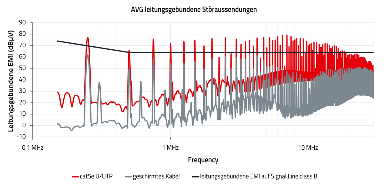
Figure 12: Conducted emission at 12 V and 2 A output current with long filtered load lines
The reason for this behavior results from the design of the isolated converter. The isolated DC/DC converter from the PoE board is connected to the digital section of the circuit without an output filter. The USB shield is connected to the digital GND. The test setup shown in Figure 13 shows that especially the shield box, which is connected to the USB cable shield, accounts for the largest dimension of the setup. The noise source of this loop is the stray capacitance of the isolated transformer. The stray capacitance from the isolated converter is the coupling path for the interference, from which the interference current flows from the switching transistor to the secondary-side switching section of the converter (digital section) and then couples to the reference ground (shield space) via the USB cable shield and the shield box. The return current path to the source results from the Ethernet cable and its termination using the AAN (Asymmetric Artificial Network) – 150 Ohm common-mode impedance. The voltage drop across the CDN (coupling/decoupling network) is then measured as the interference voltage. This interference current path is shown in Figure 14 and calculated for an area of 1 m² as an example.
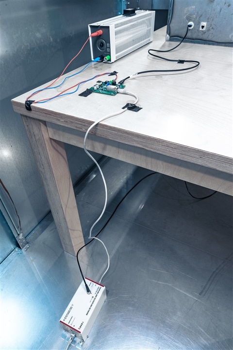
Figure 13: Test setup for conducted emission
Figure 14 shows that the impedance of the stray capacitance between the shielding box and the reference ground (wall of the shielded room) at 1 MHz is relatively high. Filtering with inductive components does not achieve an adequate solution. Instead, the stray capacitance in the test setup must be controlled. This can be achieved using a “shielding plate”, for example. However, a shielding sheet or shielding plate does not mean an RF shield, but rather a capacitive reference surface to which the board's filters can be referenced. The aim is to control the interference current circuit and prevent the interference current from flowing through the AAN.
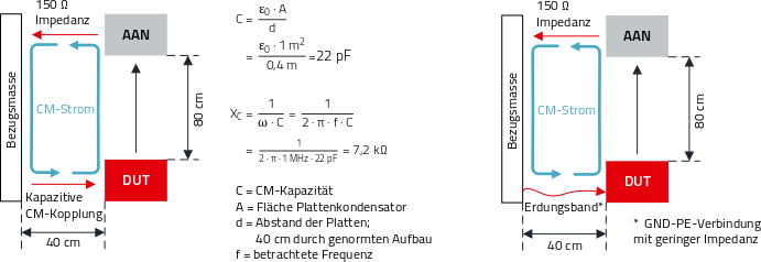
Figure 14: Interference current loop, which leads to the conducted emission
The current loop in Figure 14 increases if the secondary side of the isolated converter is connected to reference ground – via the earthing of the USB shield, for example. The interference current rises, which also increases the voltage drop in the AAN. So earthing the secondary side may cause the highest interference potential.
The situation outlined leads to the circuit diagram of the power supply on the PoE‑board as shown in Figure 2 being extended with a filter to enable compliance with the conducted emission limits. These measures result in the board setup as in Figure 15 and the circuit diagram as in Figure 3:
- A copper plate is mounted as reference ground under the board and is connected to the Ethernet cable shield.
- The input filter of the DC/DC converter at the diode bridge of the PoE connector is extended: a. 744222 common-mode choke 1 mH. b. 150 nF, 100 V (MLCC 885012208119) between VCCin and GNDin. c. Ferrites are kept. d. 4.7 nF, 2 kV (MLCC 885342211008) to the shield plate.
- An additional 4.7 nF, 2 kV coupling capacitor (MLCC 885342211008) between the primary and secondary GND is used in parallel with the transformer. The stray capacitance of the transformer is relatively high and an even larger capacitor could be used.
- The USB cable shield is connected directly to the GND plane and to the shield plate using a 4.7 nF, 2 kV capacitor (MLCC 885342211008).
The capacitor for short-circuiting the primary and secondary GND planes should in principle be significantly larger (typ. 100x) than the stray capacitance of a transformer. Given an isolation voltage of 2 kV, this becomes difficult with larger stray capacitances, so care should generally be taken with isolated power supplies and converters to ensure low stray capacitance of the transformer between the primary and secondary sides.
The optimized EMC test results are discussed in detail in chapter 4.
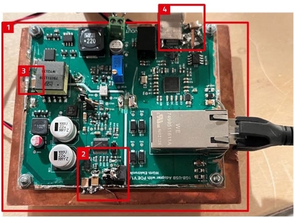
Figure 15: Extension of the board with copper sheet as the shielding plate and filter components
Note on this section: The filter measures adopted are only necessary because of the isolated voltage supply. Other optimizations here could include reducing the transformer stray capacity or applying the island concept (see chapter 05). Complex filtering of the isolated DC/DC converter is not absolutely necessary for compact devices without long secondary-side interfaces (USB and output voltage) connected, as the secondary side is small and so the radiation and capacitive decoupling will be lower.
3.5 Performance criteria for immunity testing
The performance criteria of the Gigabit Ethernet interface can be adopted for this board and only have to be extended to include stability of the power supply.
Figure 16 shows monitoring of the error and data rate over the test period. As a result of the correction and control bits used in the Ethernet protocol, around 850 MBps can be transmitted unimpaired while the notebook runs at maximum performance. Table 1 below presents the performance criteria. The additional PoE switch causes drops in speed that cannot be attributed to external interference. If these malfunctions occur during the test (marked in red in Figure 16), the corresponding frequency points must be retested. Only then is it possible with an exposure time of 3 seconds to discern whether the speed reduction is caused by interference or by effects in the auxiliary equipment, such as the PoE switch. Voltage limits of Vout +/-0.5 V are assumed to be acceptable for checking the DC/DC converter. Selection of the exposure time is described in the next chapter 3.6.
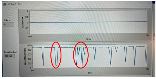
Figure 16: Monitoring of transmission speed and fluctuations due to the PoE switch
The immunity tests showed that the Ethernet interface either runs at full performance or, if influenced, drops immediately to between 20 MBps and 50 MBps or the communication fails completely. The cause for this is the very effective error correction in the Ethernet protocol, which works in different layers to detect and correct multiple errors up to almost 100%. A camera pointed at the notebook connected for monitoring allows the performance of the DUT (device under test) to be effectively monitored.
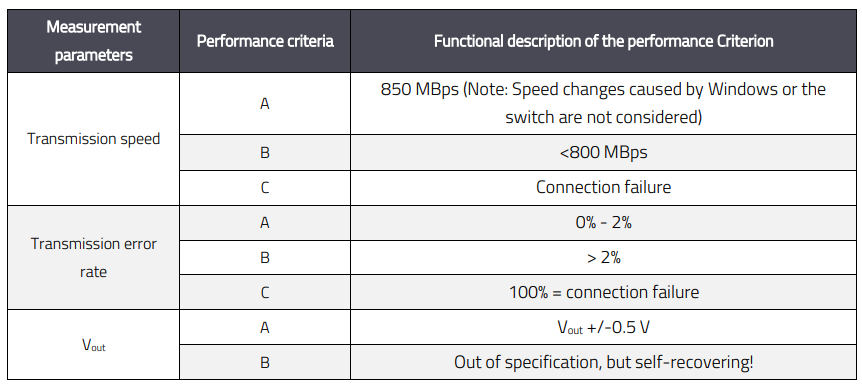
Table 1: Performance criteria of the DUT during the immunity test
3.6 Measurement time, emission test and exposure time during immunity test
The data transfer defined by the LabView software from a data string for transfer and error rate measurement leads to a viewing time of two seconds: one second error rate, one second velocity. To reliably measure both states in terms of emission as well as immunity, an emission measurement time and an exposure time of three seconds are selected for the continuous interference, as with the Gigabit Ethernet design previously.
04. EMC BEHAVIOR OF THE REFERENCE DESIGN
The setups for EMC testing shown in the next chapter are presented, among others, in Application Note ANP105 and are therefore not discussed in detail in this App Note. The EMC performance of the RD022 reference design in emission and immunity testing is present as follows. Appendix A and Appendix B also discuss and show the test results for emission with reduced filters and without optimization measures. The immunity tests were performed without adding the filter components from chapter 3.4.
4.1 Conducted emission – CISPR 32
For improved clarity in the conducted emission, only the average limit is compared with the corresponding measurement results in the average detector. As the quasi-peak detector is set to the average, the 10 dB higher quasi-peak limit is thus complied with.
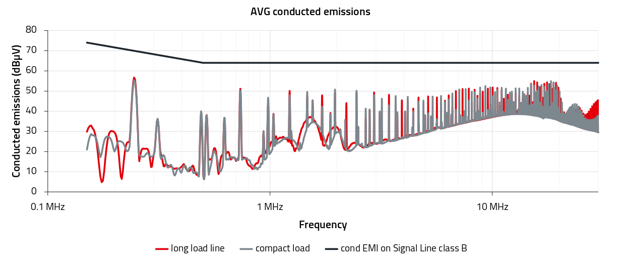
Figure 17: Conducted emission for the design in Figure 3 with unshielded cat5e U/UTP Ethernet cable at a 12 V output voltage
Following the measures presented in chapter 3.4, the measurements from Figure 17 and Figure 18 showed the design to be 9 dB below the mean limit and more than 15 dB below the CISPR 32 Class B quasi-peak limit for network cables. The emission of the shielded and unshielded cables are comparable and by changing the load from a long cable with filter to a compact load there was only a small effect on the emission in the frequency range above 10 MHz.
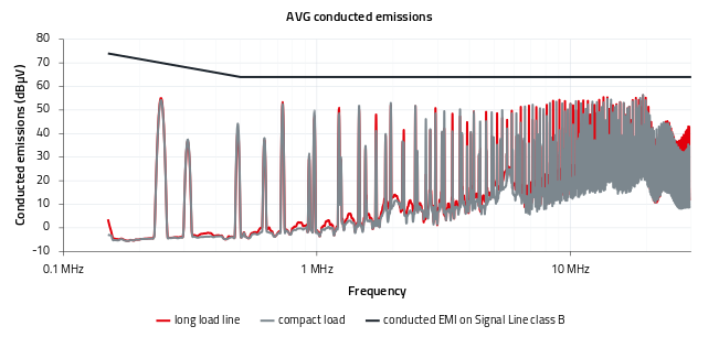
Figure 18: Conducted emission for the design in Figure 3 with shielded cat5e SF/UTP Ethernet cable at a 12 V output voltage
The measurements performed here were made with an unearthed secondary ground plane. The USB cable shield is connected directly to the digital board GND and the shield box. Coupling to the reference ground is therefore predominantly capacitive via the shield box. This application seems to realistically represent an actual PoE application, as secondary-side earthing, for example through an access point, is not useful. If the reference design with secondary-side earthing is used, additional filters need to be provided, depending on the overall system.
4.2 Radiated emission – CISPR 32
In the modified design, the radiated emission is lower when using a shielded Ethernet cable (see Figure 20) than the emission with unshielded Ethernet cable (Figure 19).
If unshielded cables are used, the emission is 5 dB below the limit if the compact load resistor is used, while the emission from the output filter and long output lines is lower, especially in the range above 100 MHz. Even comparatively small conducting structures like a TO-220 resistor with heat sink tend to radiate at these frequencies.
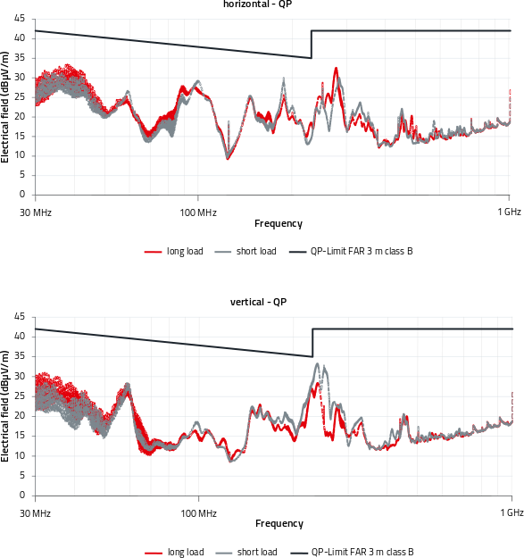
Figure 19: Radiated emission for the design in Figure 3 with unshielded cat5e U/UTP Ethernet cable at 12 V output voltage
If shielded Ethernet cables are used, the emission is slightly reduced and the levels are 9 dB below the limit. In the frequency range below 50 MHz, the more compact TO-220 resistor radiates significantly less interference. The improved performance with shielded cable reduces the difference in emission at higher frequencies. Further reduction of the radiated emission can be achieved by using a closed chassis (see Figure 30 in the appendix).
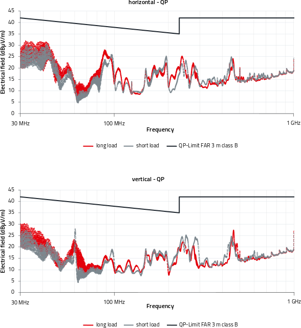
Figure 20: Radiated emission for the design in Figure 3 with shielded cat5e SF/UTP Ethernet cable at a 12 V output voltage
4.3 Radiated immunity – IEC 61000-4-3
In the radiated immunity test, performance in Criterion A could already be achieved at the maximum available field strength if shielded Ethernet cables were used in various configurations of the unmodified test board (see Figure 21):
- Long cables with filter with and without shield plate.
- Medium-length cable (was only tested without shield plate).
- Point-of-load configuration with and without shield plate.
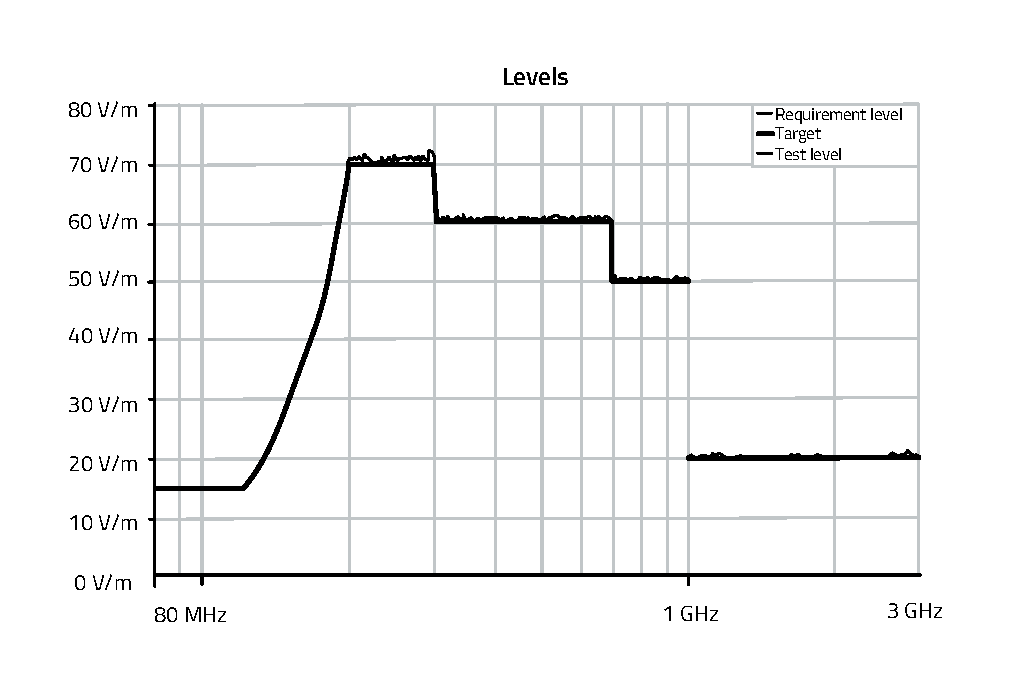
Figure 21: Maximum field strength available in the EMC lab
For unshielded cables, Criterion A could be achieved at 3 V/m. Shielded Ethernet cables are therefore suitable for high interference field strengths, while the performance using unshielded cables is not sufficient for the industrial environment.
4.4 Immunity to burst – IEC 61000-4-4
Because of some changes in the notebooks used and the use of a PoE switch, the result evaluation of the burst test is more difficult than the Gigabit Ethernet measurement series. As notebooks and switches are also partly tested, these devices also influence the result of the test.
If unshielded Ethernet cables are used, the PoE switch resets at test levels above 3 kV, which is indicated by all switch LEDs flashing. As shielding and filtering of this interference is almost impossible here, the maximum test level is restricted to 3 kV. The USB interface of the notebook resets at a test level above 3 kV. This is apparent in that all USB devices in the Device Manager disappear during the test at higher test levels. The Ethernet interface of notebooks loses its connection at 4 kV. Because of these failures, various test scenarios are undertaken for performance analysis.
- Unshielded cables: If the board is burst tested with unshielded Ethernet cables, the transmission speed is immediately reduced at already very low levels. The switch fails above 3 kV. However, from the tests with the Gigabit Ethernet board it can be deduced that the PoE board can also be operated at a higher test level in Performance Criterion B using a suitable switch.
- Shielded cables with load: The notebook, switch and load are set up openly in the test setup with the DUT. If shielded cables are tested, Performance Criterion A is achieved up to a test level of 2 kV. For an off-board temporary setup, the DUT runs very stable at comparatively high levels.
- Shielded cables without external load lines and auxiliary equipment in shield box: The load resistors also couple the burst. Coupling can go from the load resistor back to the board and therefore disturb data transfers. To test the performance of the interface at maximum test levels, a load resistor is not used in operation. This also avoids coupling of the heat sink and the board. The notebooks and the switch go in a closed shield box to which the USB cable shield and the Ethernet cable shield are connected. The setup is shown in Figure 22. Performance Criterion A was met up to a test level of 3 kV, i.e., the transmission speed was not reduced. Compared to the integrated Gigabit Ethernet board, the maximum test level in Criterion A was increased from 1 kV originally to 3 kV. The integrated PoE jack used has an improved EMC design with a two-stage common-mode filter that enhances transmission symmetry, allowing higher immunity levels. Above 3 kV, the connection remains active at reduced speed and Performance Criterion B is met.
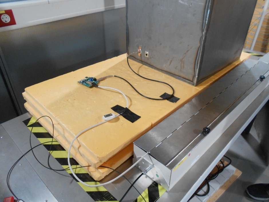
Figure 22: Setup for burst testing to determine the maximum test level
4.5 Immunity to surge – IEC 61000-4-5
Coupling the surge onto unshielded Ethernet cables was not possible due to the PoE application with the surge-high-speed CDN available. Because of the internal wiring of the CDN, operation with PoE should be possible in principle and the data sheet of the CDN also promises operation with PoE+, but it was not possible to start the DUT with surge-CDN.
If the surge is coupled to the Ethernet cable shield and using a shield plate, operation in Performance Criterion A was possible up to a test level of +/-3 kV. At higher test levels, the output voltage became unstable due to surge coupling. Undershooting of the output voltage was measured using a differential high voltage probe and is shown in Figure 23. At a test level of 5 kV, Criterion B was met in the output voltage and data communication was not affected.
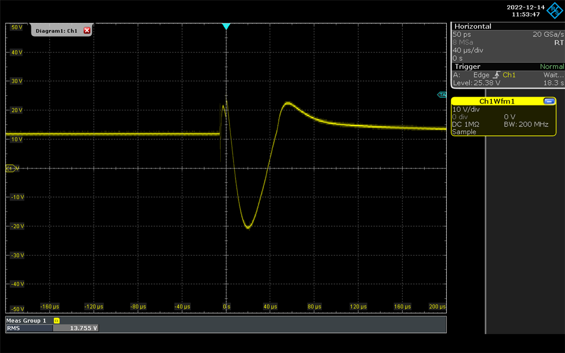
Figure 23: Oscillation at the voltage output of the DUT due to surge
This behavior can be avoided by increasing the output capacitance at the terminal. The coupled surge pulse can lead to currents of up to 2000 A at 4 kV caused by the generator impedance of 2 Ω. On the one hand, the shield and ground connections must be able to physically carry these currents, and this possibly results in oscillations in potential on the circuit board and shield plate. The current is decoupled at the shield plate and coupled on the cable shield (see Figure 24), which also affects the potential on the board due to the voltage drop of the current flow. So sufficient decoupling is required.
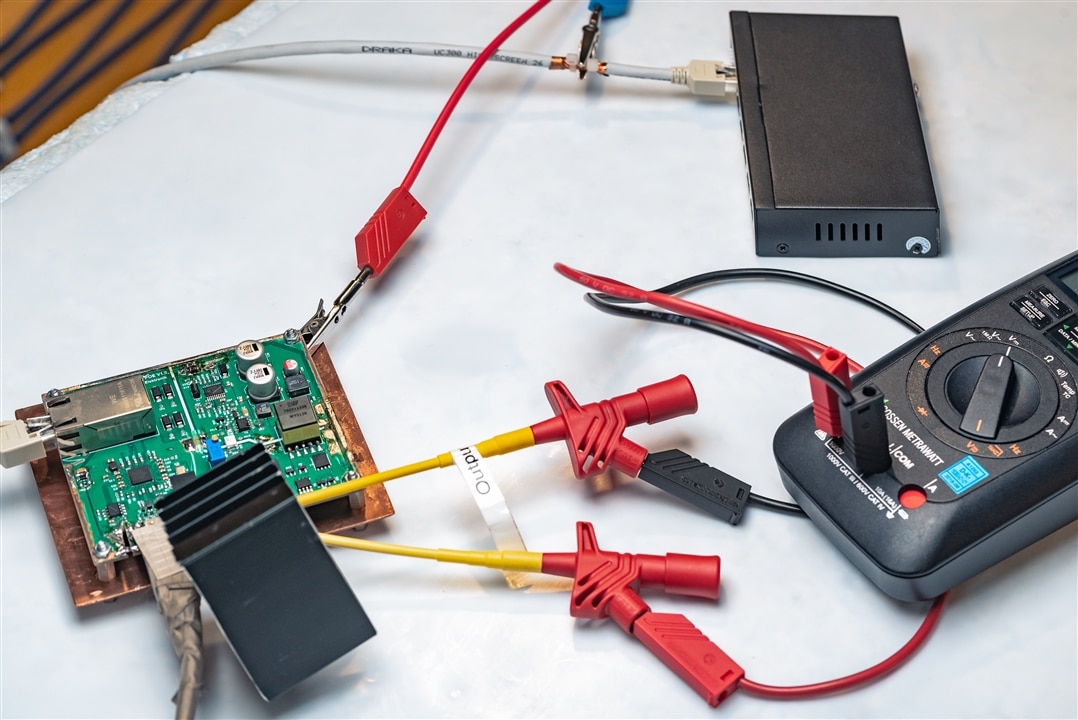
Figure 24: Surge coupling when using a shield plate.
The surge current flows through the shield plate If the surge current is decoupled directly at the Ethernet jack, this behavior is not observed and Performance Criterion A is met for voltages up to 5 kV. A possible improvement for applications with high transient voltages could therefore be a lower impedance connection between the shield GND of the board and the shield plate, together with a bigger output capacitance at the filter.
4.6 Immunity to continuous conducted interference – IEC 61000-4-6
In the conducted immunity test, performance in Criterion A could already be achieved if shielded Ethernet cables were used in various configurations of the unmodified test board with coupling at a test level of 20 V:
- Filtered long cables with and without shield plate.
- Medium-length cable (was only tested without shield plate).
- Point-of-load configuration with and without shield plate.
If unshielded cables are coupled, testing in Performance Criterion A with 10 V was possible.
05. OTHER POSSIBLE EMC IMPROVEMENTS
In emission testing, it was found that the DUT generates strong common mode interference that is attributable to the DC/DC converter. In appendix, this situation can be seen in further measurements. As shown in Figure 14, in the conducted emission test there is a common-mode interference loop whose control reduces the conducted interference. As mentioned above, the isolated DC/DC converter was identified as the source of interference. The broadband emission occurs both in the frequency range below 30 MHz as well as in the frequency range above 30 MHz. The isolated DC/DC voltage converter generates a common-mode interference potential on the entire reference ground (VCC, GND) of the assembly and all the lines and cable shields connected become antennas radiating this interference.
If the interference potential of the converter cannot be reduced by circuitry, the interference of the isolated converter must remain local and coupling to the ground plane of the board must be avoided. For interferers with such a high interference potential, the island concept can be an approach, for example. In this case, interference sources are isolated from the rest of the board and are only connected to other circuit parts via signal isolation or filters – as quasi-isolated functional components with defined interfaces. The island concept leads to the use of split GNDs. This type of board layout is not generally recommended – but can be useful in special cases, such as the DC/DC converter used here. The most important rule in the island concept is that traces must never cross a GND split and different islands and GND areas must not overlap. The islands are connected with transformers (for example optocouplers or magnetic transformers) or with EMC filters. The input and return currents are routed together here as a differential pair and then connected from one island to the next using EMC filters. This also means that implementation of the concept must take into account input and return current in the design of the board. Within the islands, the PCB design follows conventional layout rules. The following figure shows a possible island structure for the Gigabit PoE board.
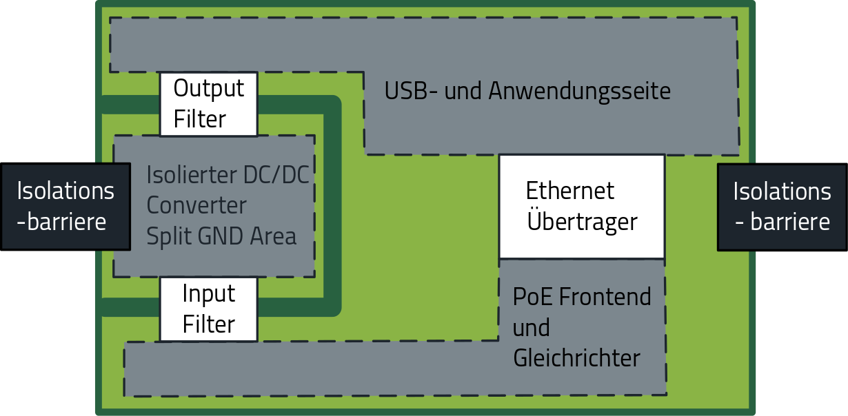
Figure 25: Island concept for the Gigabit PoE board
Figure 25 shows that signal separation already takes place during transmission at the isolation barrier and that the wanted signals are transmitted differentially. This is achieved by the transformer in the DC/DC converter and the transformers in the Ethernet jack. As a change to the existing design, only the ground layers on the DC/DC converter primary and secondary side are separated from the rest of the board. The input voltage and output voltage are separated from the PoE rectifier (input voltage) or the digital GND (output voltage) with an EMC filter. A possible filter has already been developed for the EMCoptimized design from Figure 3. A similar filter at the output can then isolate the board digital GND from the converter output voltage, which is subject to high interference.
These measures result in higher filtering and space requirements in the design, but in the case of large devices they can significantly reduce emission. The island concept is not only applicable for this circuit, but also generally for other applications. Especially for isolated converters, it can provide solutions for otherwise almost uncontrollable emission. It should be mentioned again at this point that lines on the board must never cross slots in an uncontrolled manner and transmission with EMC measures must either be differential or by use of another transformer.
Alternatively, to reduce the common-mode coupling in the DC/DC converter, a transformer with lower stray capacitance can be used, or the frequency of the interference that causes common-mode interference with the stray capacitance can be reduced.
06. SUMMARY
The results of the design were outlined for the emission measurements and compared to current limits in residential areas. If the subsequently used device with PoE interface takes on larger dimensions, or the secondary side is earthed, additional filtering is needed for the conducted emission. The emission, which is both conducted and radiated, is dominated by the isolated converter and the emission of the digital part of the circuit is negligibly low.
To reduce the emission of the converter, the island concept presented in chapter 05 can be used, and thus the interference from the isolated switching regulator can be better controlled.
Especially in immunity to bursts, the performance of the integrated PoE jack with HPLE (High Performance Low EMI Series) is improved compared to normal integrated Gigabit Ethernet jacks or toroidal transformers. This is attributable to the EMCoptimized design of the transformer with common-mode chokes on both sides and the resulting enhanced symmetry of the differential signal. If no external load were used, bursts of up to 3 kV in Performance Criterion A could be achieved with the PoE interface.
The results of the relevant tests carried out are summarized in Table 2.
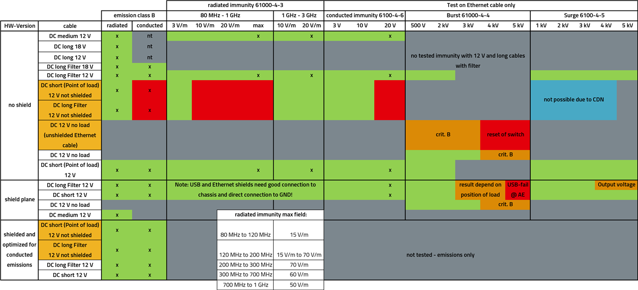
Table 2: EMC test matrix for the Gigabit PoE measurement campaign
During EMC testing, the USB interface proved to be susceptible to interference, especially during immunity testing, and a direct shield connection from the USB jack to the ground plane of the board was absolutely essential for good performance of the USB 3.1 interface.
A Appendix:
A.1 Further emission testing, design modifications, radiated emission
This appendix shows various effects in the board’s radiated emission, with the board operating with the original input filter. The findings can also be used to modify comparable products with isolated converters.
Reduction of radiated interference on the output line using a ferrite
Even short output lines can act as an antenna and radiate interference. The board is operated with short load lines and an adjustable high-load resistor. Using a snap ferrite 74271222, the common-mode currents on the load line are reduced and the emission is reduced as shown in Figure 27.

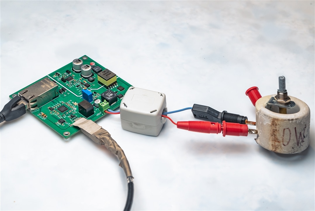
Figure 26: Operation of the board with left: medium-length load lines and right: filter using a ferrite
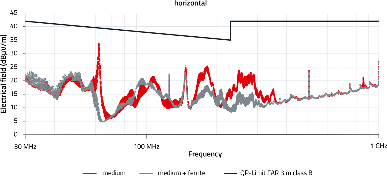
Figure 27: Radiated emission from the original design in Figure 2 with a shielded cable and 12 V output voltage
Influence of the Ethernet cable shield
From Figure 28, it can be seen that the use of an unshielded Ethernet cable significantly increases the emission.
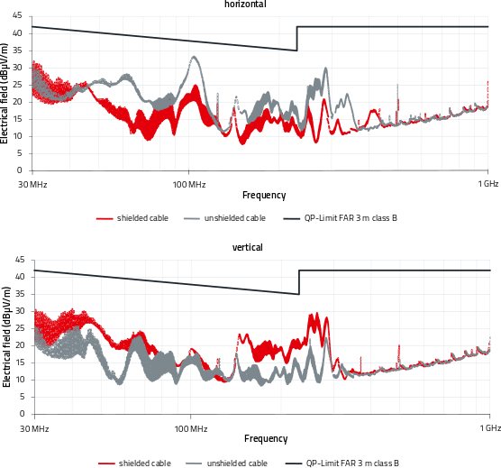
Figure 28: Radiated emission for the design in Figure 2 with long load lines and filter at 12 V output voltage
If the load with long lines and filter is replaced by a compact resistor with heat sink, the radiated emission does not improve. As no output filter is used with the compact load, the emission even increases at some frequencies.
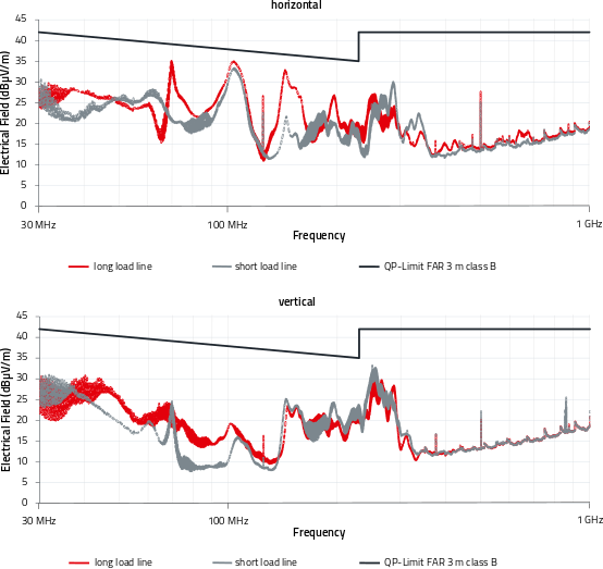
Figure 29: Radiated emission for the design in Figure 2 with unshielded cat5e U/UTP Ethernet cable at 12 V output voltage
Shield plate/ chassis
Figure 30 shows that with additional ground connection using adhesive copper tape as in Figure 31, the emission is significantly reduced. Even a slight extension of the shield plate can therefore significantly reduce emission. So, an extension to a metal case can reduce emission.
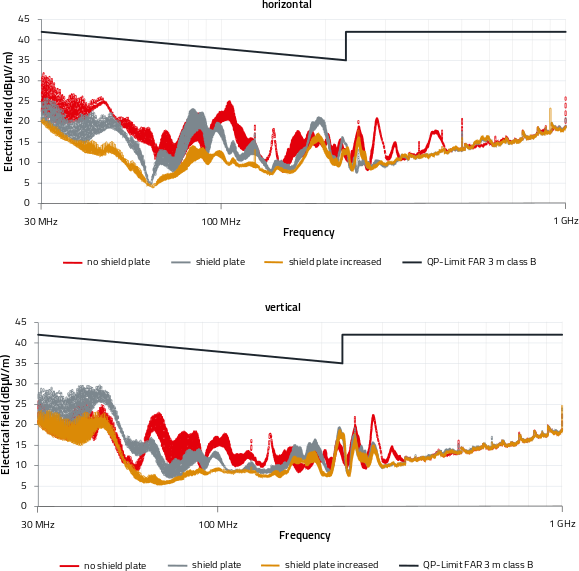
Figure 30: Radiated emission from the design in Figure 2 with a shielded cable and 12 V output voltage
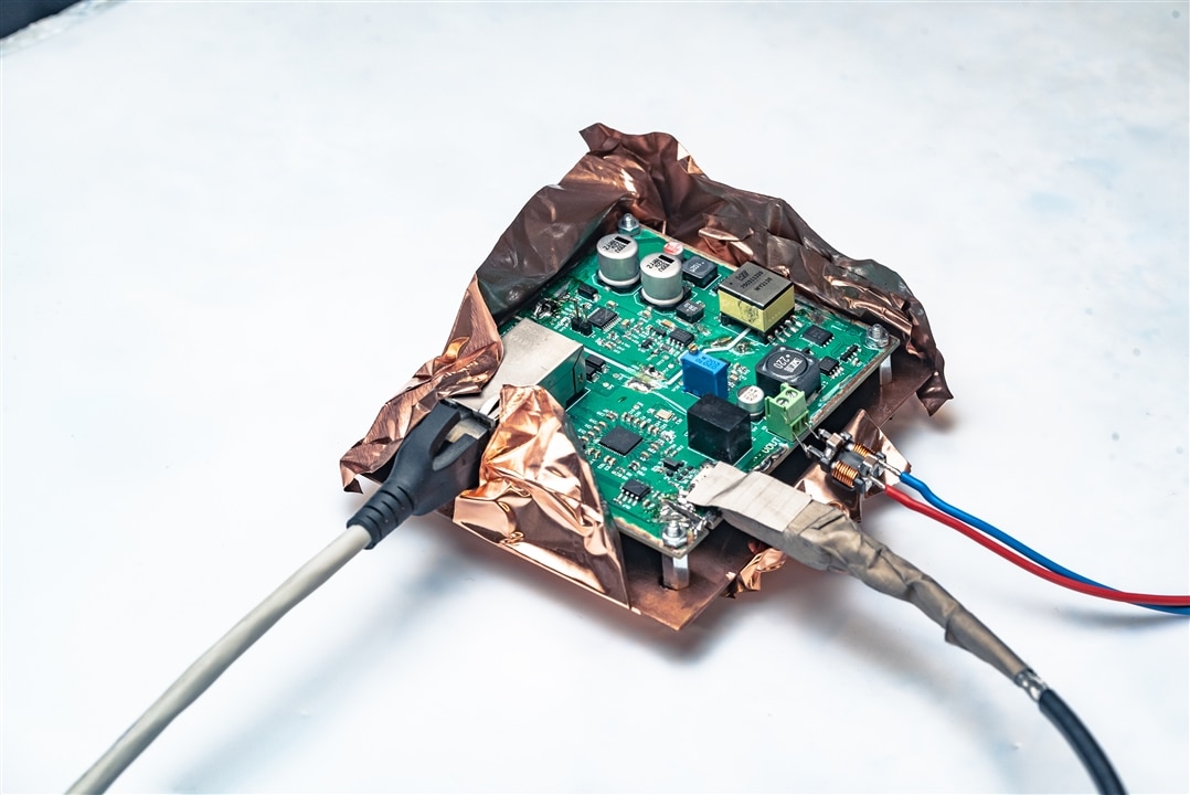
Figure 31: Extension of the shield plate with copper adhesive tape
If a chassis is used, the load should also be placed inside the shield, or lines leaving the chassis must be provided with the appropriate filters. In the results from Figure 33 in the test setup from Figure 32, the chassis reduces the interference if the load is placed on the shield plate, or a filter is used for long lines. If medium-length lines are used without filters, the emission increases.

Figure 32: Test setup with different loads and chassis plate
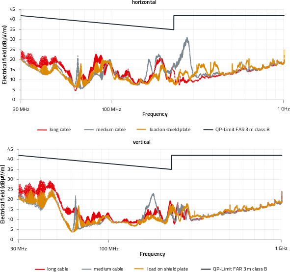
Figure 33: Radiated emission from the design in Figure 2 with a shielded Ethernet cable and 12 V output voltage
A.2 Further emission testing, design modifications, conducted emission
This appendix shows various effects of the board’s conducted emission, with the board operating with the original input filter. The findings can also be used for comparable products with isolated converters. Only the average detector is shown below, as quasi-peak and average have almost the same level in the measurement of the test board at hand. As the average limit is 10 dB lower, this is used for comparisons to obtain a better overview.
Influence of the output voltage and load on conducted emission
The board is operated with shielded Ethernet cable and long load lines with filter. The influence of the output voltage on the conducted interference on the Ethernet cable shield is shown in Figure 34. In the frequency range above 10 MHz, the interference is higher when operating with 12 V output voltage. In the range below 10 MHz, the interference spectrum is comparable.
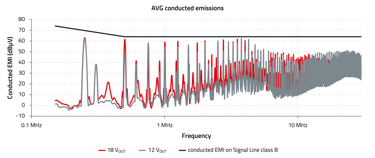
Figure 34: Conducted emission of the board according to Figure 2 with shielded Ethernet cable and long output lines with filter
If the long load line with filter used in the measurement from Figure 34 is replaced by a compact point of load (resistor), the result is the emission from Figure 35. In the frequency range above 15 MHz, the interference is slightly lower in the compact setup. A large part of the interference is output from the USB cable shield and the shield box. So the load is not part of the relevant coupling path.
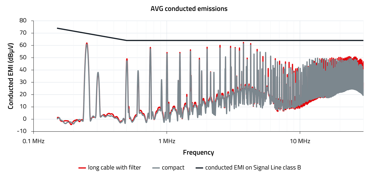
Figure 35: Conducted emission from the board in Figure 2 with a shielded Ethernet cable at 12 V output voltage
Conducted emission if an unshielded Ethernet cable is used
It was shown in Figure 12 that conducted interference increases strongly if an unshielded Ethernet cable is used. However, the influence of the load coupling path is not essential in this test either as Figure 36 shows. The interference is only slightly reduced if a compact load is used and the coupling path via the USB cable predominates.
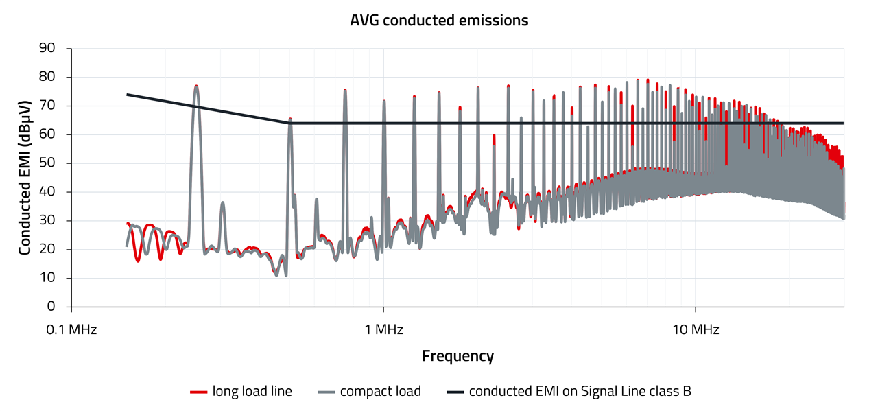
Figure 36: Conducted emission from the board in Figure 2 with an unshielded Ethernet cable at 12 V output voltage
Conducted emission if a shielded Ethernet cable and a shield plate are used
The conducted emission on the shielded Ethernet cable can be significantly reduced with a coupling plate, as Figure 37 shows. The long output lines with filter are effectively decoupled from the interference path by the filter. In Figure 38 , the filtered load with long lines is exchanged for the compact load with heat sink and the emission increases even though the coupling structure has become smaller. Whenever lines leave the shield plate, the emission increases if no suitable filter is used.
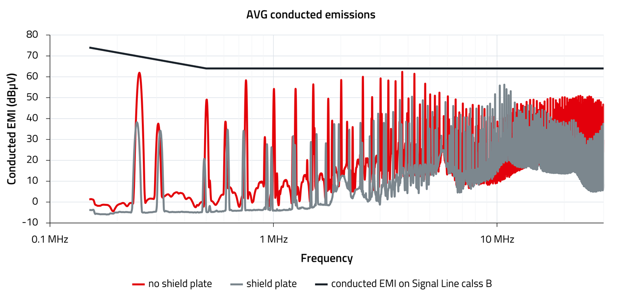
Figure 37: Conducted emission from the board in Figure 2 with a shielded Ethernet cable at 12 V output voltage
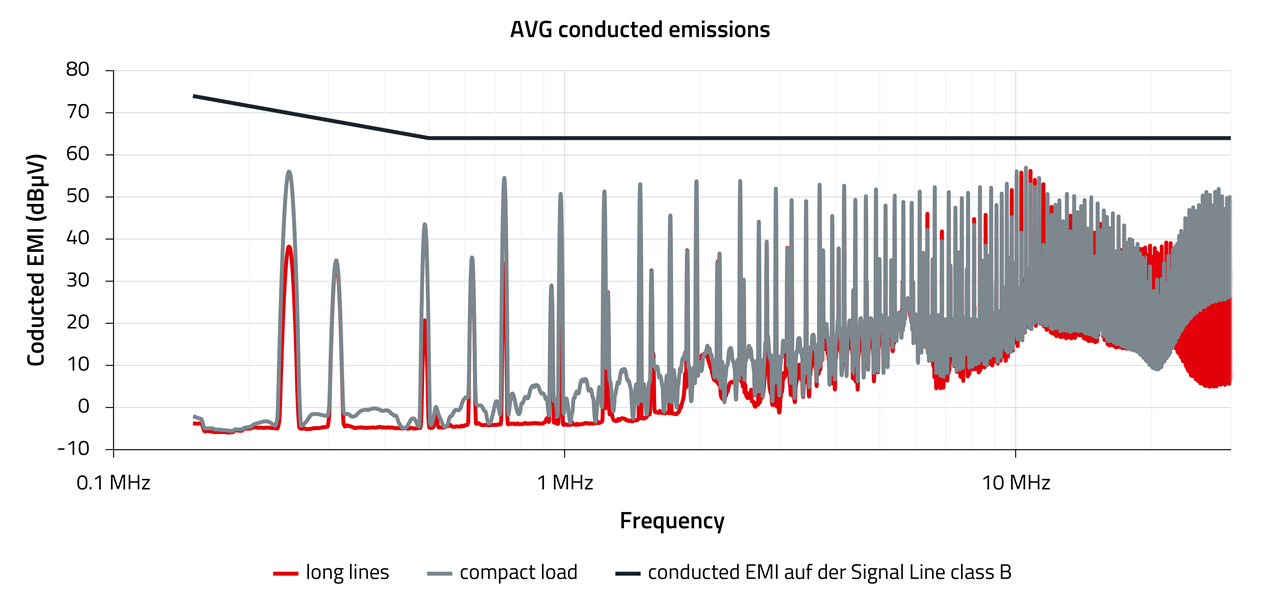
Figure 38: Conducted emission from the board in Figure 2 with a shielded Ethernet cable at 12 V output voltage and an additional shield plate
IMPORTANT NOTICE
The Application Note is based on our knowledge and experience of typical requirements concerning these areas. It serves as general guidance and should not be construed as a commitment for the suitability for customer applications by Würth Elektronik eiSos GmbH & Co. KG. The information in the Application Note is subject to change without notice. This document and parts thereof must not be reproduced or copied without written permission, and contents thereof must not be imparted to a third party nor be used for any unauthorized purpose. Würth Elektronik eiSos GmbH & Co. KG and its subsidiaries and affiliates (WE) are not liable for application assistance of any kind. Customers may use WE’s assistance and product recommendations for their applications and design. The responsibility for the applicability and use of WE Products in a particular customer design is always solely within the authority of the customer. Due to this fact it is up to the customer to evaluate and investigate, where appropriate, and decide whether the device with the specific product characteristics described in the product specification is valid and suitable for the respective customer application or not. The technical specifications are stated in the current data sheet of the products. Therefore the customers shall use the data sheets and are cautioned to verify that data sheets are current. The current data sheets can be downloaded at www.we-online.com. Customers shall strictly observe any product-specific notes, cautions and warnings. WE reserves the right to make corrections, modifications, enhancements, improvements, and other changes to its products and services. WE DOES NOT WARRANT OR REPRESENT THAT ANY LICENSE, EITHER EXPRESS OR IMPLIED, IS GRANTED UNDER ANY PATENT RIGHT, COPYRIGHT, MASK WORK RIGHT, OR OTHER INTELLECTUAL PROPERTY RIGHT RELATING TO ANY COMBINATION, MACHINE, OR PROCESS IN WHICH WE PRODUCTS OR SERVICES ARE USED. INFORMATION PUBLISHED BY WE REGARDING THIRD-PARTY PRODUCTS OR SERVICES DOES NOT CONSTITUTE A LICENSE FROM WE TO USE SUCH PRODUCTS OR SERVICES OR A WARRANTY OR ENDORSEMENT THEREOF. WE products are not authorized for use in safety-critical applications, or where a failure of the product is reasonably expected to cause severe personal injury or death. Moreover, WE products are neither designed nor intended for use in areas such as military, aerospace, aviation, nuclear control, submarine, transportation (automotive control, train control, ship control), transportation signal, disaster prevention, medical, public information network etc. Customers shall inform WE about the intent of such usage before design-in stage. In certain customer applications requiring a very high level of safety and in which the malfunction or failure of an electronic component could endanger human life or health, customers must ensure that they have all necessary expertise in the safety and regulatory ramifications of their applications. Customers acknowledge and agree that they are solely responsible for all legal, regulatory and safety-related requirements concerning their products and any use of WE products in such safety-critical applications, notwithstanding any applications-related information or support that may be provided by WE. CUSTOMERS SHALL INDEMNIFY WE AGAINST ANY DAMAGES ARISING OUT OF THE USE OF WE PRODUCTS IN SUCH SAFETYCRITICAL APPLICATIONS
DIRECT LINK
ANP122 | Gigabit PoE Interface from an EMC perspective
USEFUL LINKS:
Application Notes : https://we-online.com/en/support/knowledge/application-notes
Services: https://we-online.com/en/products/components/service
Contact : https://we-online.com/en/support/contact
CONTACT INFORMATION
Würth Elektronik eiSos GmbH & Co. KG
Max-Eyth-Str. 1, 74638 Waldenburg, Germany
Tel.: +49 (0) 7942 / 945 – 0
Email: appnotes@we-online.de

