APPLICATION NOTE
ANP124 | Capacitive Power Supplies: Selecting the Input Capacitor
ANP124 by Jon Izkue Rodriguez
The technical issues presented in this document are purely academic and are not intended to be implemented as a finished circuit in hardware. Furthermore, legal requirements for circuits that are supplied/operated with mains voltage have been disregarded in the considerations and conclusions
SAFETY WARNING
- The circuits studied and proposed in this document are directly connected to mains voltages (120 Vac / 230 Vac). Mains voltages are considered as hazardous voltages that can lead to death if touched directly. Circuits that are directly connected to mains therefore have to be handled with extreme precaution during testing and handling. Only a skilled person (according to IEC 62368-1) should operate with mains line voltage.
- Transformerless circuits that are directly connected to mains or hazardous voltages do not provide any kind of safety isolation to protect against electric shock. It is mandatory that the upstream supply circuit of a transformerless circuit as described in this document ensures a safeguard as described in the IEC 62368-1.
- Designing electrical hardware intended for mains voltage, such as 120 Vac / 230 Vac, entails inherent risks and responsibilities. It is necessary to observe and adhere to industry standards, and prioritize safety throughout the entire design process.
- By engaging in the design and implementation of electrical hardware for mains voltage, you acknowledge and accept the responsibility for ensuring the safety and compliance of your design. The section "IMPORTANT NOTICE" at the end of this document is mandatory to read before starting.
01. INTRODUCTION
A capacitive power supply is a very low-cost AC/DC converter without a transformer or switching components. With a very small parts count, these circuits can provide a DC voltage for low-power applications. In addition, because no high-speed switching is occurring, no EMI noise is generated. Transformerless power supplies are widely used in lowpower applications connected to mains power where isolation is not required. Yet many circuit developers are unfamiliar with this AC/DC converter topology. There are several names of similar circuits: capacitive power supplies, capacitive droppers, and transformerless power supplies. Since the output is not galvanically isolated from the mains voltage, the range of possible applications is reduced. The recent interest in technologies for IoT (Internet of the Things) and Smart-Home have expanded the use of low-cost low power (< 1 W) power supplies e.g. needed for Smart devices like light switches or power meters and ambient sensors (temperature, light) for smart home applications. The critical design component in a capacitive power supply is the input capacitor. In theory class X2 capacitors are electrically suited for that but this is not the intended use of X2 capacitors as defined by IEC-60664-1. Many capacitor manufacturers do not recommend X2 capacitors for these applications, while some permit the use or offer alternative series for capacitive power supply. We will investigate the reasoning for that in this document.
02. FROM VOLTAGE DIVIDER TO POWER SUPPLY
Although this topology is not as well-known as other alternative solutions, its basic concept relies on one of the most familiar concepts in electrical technology: The voltage divider (Figure 1).
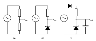
Figure 1: Voltage divider for mains AC voltag
2.1 Connecting a voltage divider to line voltage
In the following analysis, we will assume the power extracted from Vout, understood as the target load, will be small enough to have a negligible impact on the rest of the circuit. The circuit in Figure 1(a) is hardly of any use. The voltage in Vout will be as low as desired, but it will still be AC and to extract any useful power, much more power will be dissipated and wasted in the resistors. If we replace the lower resistor with a Zener diode rated for the desired voltage, as shown in Figure 1(b), we will get the desired voltage in Vout at least every half cycle. However, during the other half of the cycles, Vout will be 0 V and we will still lose most of the power in the resistor that takes the burden for most of the voltage. If we complete the circuit as shown in Figure 1(c), we will have a usable circuit for our target Vout. The diode in series will provide only the voltage of the positive half-wave and the capacitor connected parallel to the Zener diode will provide for the necessary DC voltage smoothing at Vout. Thanks to the rectifier diode, the capacitor will not be discharged during the negative half wave, provided the power output is low enough for the selected capacitance. This circuit is simple and works as intended, but it is not viable due to its very low efficiency.
2.2 Capacitive voltage dropper
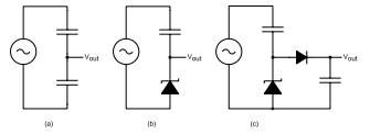
Figure 2: Capacitive voltage divider
How can we improve the circuit? Since we are working in AC, we can replace the resistors in the voltage divider with capacitors as shown in Figure 2(a). The impedance of an ideal capacitor is only the reactance![]() . For example, a 100 nF ideal capacitor at 50 Hz will have about Zideal@50Hz = X@50Hz = 31 831 Ω. We can call this a capacitive dropper circuit. The reactance of the capacitor is taking the burden of the voltage so we are not dissipating energy like in the resistive voltage divider. Using a Zener diode as in Figure 2(b) we obtain the rated Zener voltage during half of the period, as discussed previously. This is an AC voltage from 0 V to Zener voltage peak, and we only need to rectify it to obtain the output DC voltage. Finally, in Figure 2(c) we add the rectifier diode and an output capacitor to get the expected DC voltage output. If you paid attention, you may have noticed that we placed the rectifier in a different place than in the resistive example. This is necessary because the voltage divider built with capacitors will only work with AC voltage. To work as intended, the capacitor needs to operate in AC, in other words, it must be able to charge and discharge following the mains voltage in both positive and negative half cycles.
. For example, a 100 nF ideal capacitor at 50 Hz will have about Zideal@50Hz = X@50Hz = 31 831 Ω. We can call this a capacitive dropper circuit. The reactance of the capacitor is taking the burden of the voltage so we are not dissipating energy like in the resistive voltage divider. Using a Zener diode as in Figure 2(b) we obtain the rated Zener voltage during half of the period, as discussed previously. This is an AC voltage from 0 V to Zener voltage peak, and we only need to rectify it to obtain the output DC voltage. Finally, in Figure 2(c) we add the rectifier diode and an output capacitor to get the expected DC voltage output. If you paid attention, you may have noticed that we placed the rectifier in a different place than in the resistive example. This is necessary because the voltage divider built with capacitors will only work with AC voltage. To work as intended, the capacitor needs to operate in AC, in other words, it must be able to charge and discharge following the mains voltage in both positive and negative half cycles.
2.3 Completing the capacitive power supply design
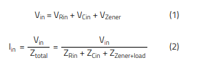
We have now an operating AC/DC converter with only four components, and it is much more efficient (at least compared with the previous resistive options). This design should be improved with small changes to make it more efficient and work reliably in real applications. If we replace the simple rectifier diode with a full bridge rectifier, we will be using both positive and negative half cycles. As we will see later, this allows us to dimension an input capacitor with half of the capacitance previously required for the same output current. The voltage divider (assuming the ideal rectifier) would be (as in Figure 3)
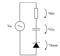
Figure 3: Final voltage divider
There are also advantages to be considered regarding the placement of a resistor in the input line. If we connect a relatively big input capacitor to the grid power, it may draw so much current in the first charging cycle that it could trip a circuit breaker. High-power mains power supplies with large input capacitance deal with this by building complicated softstart circuits, but that is nothing we can afford if we want to keep the design simple and low cost. A simple input resistor provides the necessary inrush current limitation. This resistor will cause additional power loss, but it is a necessary protection and if correctly dimensioned it will only dissipate and waste a reasonably small amount of power.
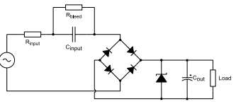
Figure 4: Simple capacitive power supply
Finally, we will add a high-ohm resistor parallel to the input capacitor. As always with AC-mains-connected circuits, the safe discharge of the input capacitor must be guaranteed. This is a safety feature and it will have a negligible effect in the performance of the circuit. In Figure 4 we have rearranged the circuit in the most common configuration of this topology.
03. DESIGNING AN EXAMPLE CAPACITIVE POWER SUPPLY
The main design parameter in the converter is the input capacitor. The capacitance of the input capacitor will determine the maximum output current, (almost) independently of the output voltage. In the following steps, we will calculate the output current.
First, we assume the resistance in parallel to the input capacitor (see Figure 4) is high enough so that we can ignore its effect when we calculate the current flowing in the input capacitor:

In order to calculate the maximum current available to the load, we need to calculate first the input RMS current. Ignoring the forward voltage drop across the rectifier diodes, we have:

The |Zin| term represents the modulus of the combined impedance of the input capacitor and series resistor, ignoring the discharge resistor parallel to the capacitor, we obtain:

The maximum DC current available to the load corresponds to the average value of the fully-rectified input current calculated above, as follows:

And with the amplitude of the AC current we get finally:

The load should be designed in such a way that the load current can never be higher than this value otherwise the voltage at the output will collapse. The low combined impedance of the system formed by the Zener diode, output capacitor, and load is the cause of this collapse. Now the designers have to understand, that this output current will be available for the load if necessary, but will always “flow” through the capacitor due to the voltage divider. Therefore, the remaining current will flow through the Zener diode. The total output DC current through the capacitor will remain constant independently of its distribution between the Zener diode, output capacitor, or load.
3.1 Calculate the input resistor
The input series resistor is only necessary to limit the inrush current when the power is connected and the series capacitoris discharged (or in the worst case, charged with inversed polarity). In the beginning, the capacitor acts like a short to the mains voltage and without the series resistor, an inrushcurrent of several hundred amperes could flow in the circuit and damage the capacitor or the rectifier diode. To calculate the resistor, we can calculate the inrush current with

However, the series resistor will cause power dissipation at all times during the converter operation. This is the reason why high-power AC/DC converters have a complex softstart/bypass system to bypass the current limitation in normal operation. Such a system is not necessary in this design, because the low power of the converter will keep those losses small. The power dissipation can be calculated with the formula:

It is easy to plot both formulas to find a tradeoff between the steady-state power dissipation and a desired safety current limitation. If we consider an output current of 20 mA in this example, we get a graph like shown in Figure 5.
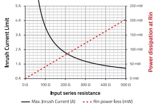
Figure 5: Input resistance selection, calculated for Iout,max = 20 mA
Finally, the designer must consider the physical size and construction of the resistor, using the calculated rated power. Leaded (THT) resistors may be advantageous here regarding power dissipation and advantages in mains voltage circuits, such as increased clearance distances and surge protection. In our circuit, we built 300 Ω with leaded resistors and the inrush current will be under 1.1 A in the worst case.
3.2 Choosing the input capacitor
From the previous calculations, we see that the input capacitance will directly limit the output power. The input resistor will reduce the output current, too. However, we have already calculated Rin with only safety considerations. For example, if we use a 330 nF input capacitance as well as 300 Ω resistance, we can calculate with the formulas above, the available maximum output current of 20 mA.
There are other requirements for the input capacitor:
1. The input capacitor must be rated for AC mains voltage.
2. Capacitance variation due to operating voltage and temperature must be very low to keep the available load current stable.
3. Capacitance drop during the lifetime of the capacitor must also be kept very low.
For most applications with this topology, the input capacitance will be between 100 nF and 1000 nF. Given those requirements, AC Film Capacitors with Polypropylene dielectric film (also called MKP capacitors) are most commonly used. Ceramic capacitors (like MLCCs) with the appropriate voltage rating could also be used. Class 2 ceramic capacitors are not recommended due to unstable capacitance under load, voltage and temperature.
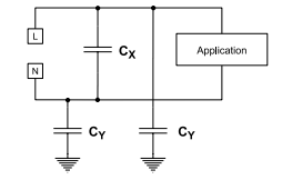
Figure 6: Connection of X and Y capacitors
Capacitors with class 1 ceramics (NP0) are therefore recommended, but it may be costly to achieve the required capacitance except in cases with extremely low load current. X2-Safety Class EMI Suppression capacitors, like our WCAPFTX2 and WCAP-FTXX film capacitor product series, as well as WCAP-CSSA multilayer ceramic capacitors are specifically built to be connected “across the line”, between line and neutral (see Figure 6). This connection is also called parallelto-mains. The load profile for the input capacitor in the capacitive power supply is similar to this application, we may benefit from the surge voltage protection and self-healing capabilities (see IEC 60384-14). However, many manufacturers explicitly advise against using regular X2 MKP capacitors in a “series-to-mains” application. In the capacitive power supply, the most important characteristics are capacitance tolerance and stability. Surge capabilities are of less importance because the series resistor and load impedance provide a higher impedance in series to the capacitor and the surge voltages will be reduced in comparison with the conventional X2 connection as a filter element. Some capacitor manufacturers provide a special series for this application, while others recommend “Temperature Humidity Bias” or THB Type X2 capacitors. This type of capacitor is made with metalized polypropylene film (MKP) same as conventional boxed X2 film capacitors, but they provide narrower tolerances and capacitance stability during the lifetime of the capacitors, including under high-stress conditions like high temperature and humidity. Different manufacturing materials and processes achieve this result: better quality and thicker epoxy resin, special treatment on the base film, and tight humidity control during the manufacturing process. One possible reason for manufacturers not to recommend ordinary X2 capacitors in this design is that X2-types are not specifically designed to fail open, like Y2-Class capacitors. The short-failure situation is not a problem in fuse-protected X2 applications like a line filter because the fuse will always trip in a short-circuit failure across the line. In a capacitive power supply the load and series resistor could theoretically keep the short-circuit current low enough for the fuse not to trip and still cause damage to the load or other parts eventually. This failure can also be avoided by the use of a low voltage varistor (or MOV) after the series capacitor.
3.3 Capacitor discharge resistor
A resistor is connected in parallel to the input capacitor to safely discharge it when the mains voltage is switched off. This resistor is often called a bleeder resistor. A good rule of thumb to estimate the time it takes to discharge the capacitor is to calculate the time constant of the RC network of the capacitor and resistor. After 5τ = 5 · R · C = 5 · Rbleed · Cin we expect the voltage at the capacitor to be 99% lower than the initial voltage at the start of discharge. Again, there is a tradeoff between the speed to discharge and the power loss dissipated by the resistor. To select the correct power rating of the resistor, we calculate the power loss as a permanent load of the resistor:

This is a worst case approximation with the assumption that we can ignore the effect of the Zener voltage in the voltage of the input capacitor.
3.4 Input voltage
In most European countries, the regulation specifies a mains voltage of 230 Vrms ± 10% voltage between a phase and the neutral connector. Our design example is based on this system and should be recalculated for other operating conditions. The minimum and maximum voltage values must be considered in all previous calculations to select suitable parts. For example, with the minimum possible voltage (207 V) we can calculate the minimum required input capacitance for the desired load current. On the other hand, we will have the maximum current flowing when the voltage is at the maximum possible level (253 V). With this maximum power definition, we calculate the power ratings of the components, especially the input resistor and Zener diode.

Table 1: Effects of voltage tolerance in Europe – 230 V ± 10% (50 Hz)
It is understood that the calculations will change with other mains line voltage frequencies. The engineer must consider that when calculating the tolerances. In contrast to most AC/DC switch mode power supplies (SMPS), capacitive power supplies are not appropriate for very wide input voltage ranges, like the common 100 to 240 V input of many AC/DC power supplies and wall adapters. To calculate the extreme situations, we can add the input capacitor tolerance for capacitance. For example, our used WCAP-FTXH capacitor series have 10% tolerance, so in the conditions of maximum input voltage and maximum capacitance, we have 22.2 mA. With the minimum voltage and capacitance, we will have only 14.6 mA available to supply our load.
3.5 Output capacitor
The output capacitor in this circuit is necessary to provide a stable DC voltage to the load. Depending on the load profile, more or less bulk capacitance must be added. In our design, a 100 µF capacitor leads to a voltage ripple of 0.5 V peak-topeak. Of course, a larger capacitance will delay the charging because the charging current is limited by the maximum load current. Our design with 100 µF takes about 350 ms to the stable voltage of 12 V. Any electrolytic capacitor with the correct voltage rating will be fine since the Zener diode will provide additional protection against overvoltage. Of course, other capacitor technologies like Multilayer Ceramic Capacitors (MLCC) or Polymer Electrolytic capacitors are suitable and could even provide some benefits, but we want to keep the component cost as low as possible. In this case, the cost per µF of electrolytic caps is the lowest without any drawback.
3.6 Zener diode
The Zener diode is a simple and efficient way to provide a constant voltage to our load. The calculated output current that will flow through the rectifier remains constant in operation. In the worst case of no load and charged capacitor, all the calculated output current will flow through the Zener diode. Therefore, we have our design specification for the power rating of the Zener diode:

In our calculations, we have calculated a load current that in the worst case will be around 22 mA. In operation, part of that current or all of it may flow through the Zener diode. Given also the 5% tolerance of the Zener voltage, the maximum power will be 22 mA ∙ 12.6 V = 277.2 mW. The very common DO-35 (or DO-204AH) leaded diode package has a power rating of 500 mW so this should not be a problem. If the load requires a very stable low voltage like 3.3 V for a microcontroller, it is recommended to use a Zener diode for higher voltage and a voltage regulator after the capacitor.
3.7 Line protection
Depending on the system where the power supply will be connected, some protection may be needed on the mains voltage input. In our test circuit, we used a combination of a varistor and a fuse. A varistor should be placed at the input of the circuit to shortcircuit transient overvoltages from the mains. We used disk varistors from the Würth Elektronik WE-VD Family with a rated voltage of 300 Vrms. A fuse in series with the circuit must be placed before the varistor and will provide overcurrent and overload protection for the mains if there is a failure in the capacitive power supply. X2 capacitors normally fail open, but it is theoretically possible that they fail short because they don't have the necessary design to always fail open, like Y2 capacitors do. One possible safety issue is the scenario where the input capacitor is shorted and the input resistor bears most of the AC voltage from mains. Both the fuse and the input resistor must be selected properly, taking this case in consideration.
3.8 Simulation

Figure 7: LTspice schematic
With LTspice XVII it is possible to perform various simulations to verify the calculations and compare them with momentto-moment values. We took advantage of the available LTspice libraries for most of the used components. The LTspice libraries for capacitors and LEDs are available via the Würth Elektronik eiSos webpage. We also used built-in libraries for the simulation models of the rectifier diodes (simulated as 4x regular Schottky RR1VWM6S) and the Zener diode (BZX84C24VL).
3.9 Power losses and efficiency
One strength of the simulation analysis is the ability to get better calculations of the power losses and the converter efficiency. Power functions for each component can be plotted and easily integrated for average values with the .meas directives. Before that, we can estimate the losses with the simplified calculation from the previous section. The losses at the input resistor, bleeder resistor, and rectifier are respectively:
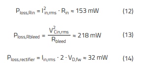
As we determined before, the load current after the rectifier will be available to the load and the rest will flow through the Zener diode. The available output power is

The required load power should be slightly below that value, to account for tolerances and the aging of the input capacitor. The power not used by the load will be dissipated as loss at the Zener diode. Then we have

In our example circuit with a load of 900 Ω (let's ignore the LED), we have an output power of 160 mW. Therefore, taking only the previously discussed losses into account we have Plosses + Pload ≈ 153 + 226 + 32 +244 ≈ 646mW, we can calculate the efficiency as:

These calculations are confirmed with the LTspice simulation. The simulation is more accurate because it provides us with the average and integrated values of the waveforms and also because we use more realistic models of the components. We also get values for the very low losses at the input and output capacitors, which are more difficult to estimate. The power efficiency can be easily improved if we look at the power losses generated at the input series resistor (Rin), the bleeder resistor (Rbleed), and the Zener Diode. The input resistance could be reduced to 100 Ω and the bleeder resistor may be increased to 470 kΩ while not considerably affecting the circuit. With these measures, we can increase the efficiency to around 40%. The power losses at the Zener diode could theoretically also be reduced, but as explained before, some amount of Zener current is necessary for the correct operation of the converter. Depending on the expected lifetime and input voltage requirements, we may even need to increase the Zener current, thus decreasing the efficiency in normal operating conditions. Another interesting calculation made in LTspice is the apparent power/reactive power and with that the power factor. We calculate a very low power factor of about 12% (capacitive), which is to be expected by looking at the load profile: as seen from the input, we can simplify the whole circuit as a capacitor and a relatively low resistance resistor (load included). With the input capacitor impedance dominating, this means that the whole system is a mostly reactive (capacitive) load. The low power factor is not an issue because the capacitive power supply power rating is not high enough for a power factor correction (PFC) to be required. The Standard IEC 61000-3-2 requires PFC for power supplies only with a power output of more than 25 W.
04. CONSTRUCTION OF A CAPACITIVE POWER SUPPLY
As with any circuit connected to line voltage, user safety must be rigorously guaranteed. It is the responsibility of the design engineer to incorporate safety considerations in the design. In this application note we will not discuss the necessary steps but we can provide an overview of the international standards that must be observed. The IEC 60664-1 Insulation coordination for equipment within low-voltage supply systems - Part 1: Principles, requirements and tests addresses in general the required clearance and creepage distances to provide necessary insulation in the design for electrical equipment. This must be considered in the layout of the PCB. Other protective devices like surge protection devices and fuses are outlined in the standard. The IEC 62368-1 Audio/video, information and communication technology equipment – Part 1: Safety requirements and the IEC 61010-1 Safety requirements for electrical equipment for measurement, control, and laboratory use - Part 1: General requirements are product specific safety standards. Both could be a base for the determination of the clearance & creepage as well as for the necessary safe guards. The corresponding chapters gives here more information about the values that should be chosen.

Figure 8: Schematic of the test board in EAGLE
05. MEASUREMENTS
5.1 Test board
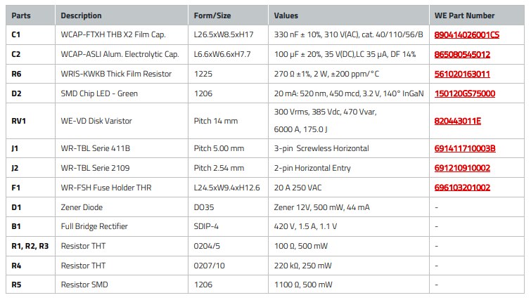
A test board was designed and assembled to test different performance configurations (see schematic in Figure 8). The Bill of Materials is included in the appendix of this document. The primary purpose of the test board was to demonstrate the usability of the circuit as a power supply. Therefore, although numerous safety measures were of course implemented, the general qualification required for end products was not implemented. To test the long term stability of the circuits, we performed a loaded test under high-stress environmental conditions as an accelerated life test. We applied 230 V (AC) to the input and placed the circuits for 1000 hours in a climate chamber at a temperature of 85 ºC and a relative humidity of 85%. These conditions are similar to the harsh damp heat tests passed by the THB-Type film capacitors. According to DIN-IEC 30485- 14 this is what qualifies the components as Environmental Grade IIIB.In our test, we used 330 nF X2 capacitors from different vendors and with and without a “series-to-mains” application rating. All capacitors approved for use in a capacitor power supply performed very well, with all of them losing less than 10% of their capacitance, most of them less than 5%. For capacitors that are not recommended for use in series with the mains, the results varied widely from -10% to -50% capacitance loss. An important conclusion from our tests is therefore that with the regular X capacitors in the application as part of the interference suppression filter, a drop in capacitance may have an only minor effect on their use, provided the filter has been designed properly. In contrast, a drop in capacitance in capacitive dropper circuits can lead to failure of the power supply unit. Due to the critical nature of capacitance degradation in this application, we recommend that our customers designing such systems perform and evaluate a wide range of accelerated lifetime measurements under load and high humidity conditions. In addition, various safety aspects and component failure mechanisms need to be analysed, not just the ageing of the capacitor.
5.2 EMC Measurement
We had the chance to use our EMC Laboratory and do a full pre-compliance EMC Test according to CISPR32. As an example, you can see the results of the conducted emission test as measured at the neutral line in Figure 9. The capacitive power supply circuit is a mostly capacitive load as seen from the input. As we expected, there are no EMC compliance issues to consider in our example circuit.
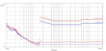
Figure 9: EMC Conducted emissions test result
06. SUMMARY
Transformerless capacitive power supplies are very low-cost and relatively easy-to-design solutions for low-power applications without the requirement of galvanic isolation. In this document, we explain their operation and design calculations.The input capacitor is the most critical component and it must be carefully selected to ensure performance and lifetime operation. As a result of our measurements, we discourage the use of regular X2-class film capacitors, like the series WCAP-FTXX and WCAP-FTX2 , in series-to-mains applications. Capacitive power supplies designed for long load life require capacitors with foils and dimensions specifically designed for this application. For its capacitance stability and ruggedness, we recommend using THB film capacitors like the Würth Elektronik eiSos WCAP-FTXH series for capacitive power supply applications. Please be aware that only some of the parts of the WCAP-FTXH series are recommended for applications in series to mains. Always check the datasheet and for any additional questions contact our sales representatives or us directly though our contact form.
07. APPENDIX
A.1 Bill of Materials – Test board
A.2 References
[1] Designer Circuits, LLC; Transformerless Power Supply Design – DesignNote 001C“
[2] Microchip, AN954 Transformerless Power Supplies Resistive and Capacitive, 2004
[3] STMicroelectronics, AN2300 Application Note, An alternative solution to capacitive power supply using Buck converter based on VIPer12A, 2006
IMPORTANT NOTICE
The Application Note is based on our knowledge and experience of typical requirements concerning these areas. It serves as general guidance and should not be construed as a commitment for the suitability for customer applications by Würth Elektronik eiSos GmbH & Co. KG. The information in the Application Note is subject to change without notice. This document and parts thereof must not be reproduced or copied without written permission, and contents thereof must not be imparted to a third party nor be used for any unauthorized purpose. Würth Elektronik eiSos GmbH & Co. KG and its subsidiaries and affiliates (WE) are not liable for application assistance of any kind. Customers may use WE’s assistance and product recommendations for their applications and design. The responsibility for the applicability and use of WE Products in a particular customer design is always solely within the authority of the customer. Due to this fact it is up to the customer to evaluate and investigate, where appropriate, and decide whether the device with the specific product characteristics described in the product specification is valid and suitable for the respective customer application or not. The technical specifications are stated in the current data sheet of the products. Therefore the customers shall use the data sheets and are cautioned to verify that data sheets are current. The current data sheets can be downloaded at www.we-online.com. Customers shall strictly observe any product-specific notes, cautions and warnings. WE reserves the right to make corrections, modifications, enhancements, improvements, and other changes to its products and services. WE DOES NOT WARRANT OR REPRESENT THAT ANY LICENSE, EITHER EXPRESS OR IMPLIED, IS GRANTED UNDER ANY PATENT RIGHT, COPYRIGHT, MASK WORK RIGHT, OR OTHER INTELLECTUAL PROPERTY RIGHT RELATING TO ANY COMBINATION, MACHINE, OR PROCESS IN WHICH WE PRODUCTS OR SERVICES ARE USED. INFORMATION PUBLISHED BY WE REGARDING THIRD-PARTY PRODUCTS OR SERVICES DOES NOT CONSTITUTE A LICENSE FROM WE TO USE SUCH PRODUCTS OR SERVICES OR A WARRANTY OR ENDORSEMENT THEREOF. WE products are not authorized for use in safety-critical applications, or where a failure of the product is reasonably expected to cause severe personal injury or death. Moreover, WE products are neither designed nor intended for use in areas such as military, aerospace, aviation, nuclear control, submarine, transportation (automotive control, train control, ship control), transportation signal, disaster prevention, medical, public information network etc. Customers shall inform WE about the intent of such usage before design-in stage. In certain customer applications requiring a very high level of safety and in which the malfunction or failure of an electronic component could endanger human life or health, customers must ensure that they have all necessary expertise in the safety and regulatory ramifications of their applications. Customers acknowledge and agree that they are solely responsible for all legal, regulatory and safety-related requirements concerning their products and any use of WE products in such safety-critical applications, notwithstanding any applications-related information or support that may be provided by WE. CUSTOMERS SHALL INDEMNIFY WE AGAINST ANY DAMAGES ARISING OUT OF THE USE OF WE PRODUCTS IN SUCH SAFETYCRITICAL APPLICATIONS.
DIRECT LINK
ANP124 | Capacitive Power Supplies: Selecting the Input Capacitor
USEFUL LINKS:
Application Notes : https://we-online.com/en/support/knowledge/application-notes
Services: https://we-online.com/en/products/components/service
Contact : https://we-online.com/en/support/contact
CONTACT INFORMATION
Würth Elektronik eiSos GmbH & Co. KG
Max-Eyth-Str. 1, 74638 Waldenburg, Germany
Tel.: +49 (0) 7942 / 945 – 0
Email: appnotes@we-online.de

