


Application Note
TVS diodes: basics, function and their applications
ANP143 by Dr.-Ing. (Doctor of Engineering) Heinz Zenkner
1. BASICS
TVS diodes (transient voltage suppressors) are used to protect circuits from high voltage spikes. They are designed to operate in reverse bias and work by discharging interference current when the reverse voltage exceeds the ‘avalanche breakdown potential’. They are essentially high-power Zener diodes and represent a special form of avalanche diodes. TVS diodes can withstand large power spikes (hundreds or thousands of watts), but Zener diodes have a narrower voltage tolerance. TVS diodes generally have a higher parasitic capacitance than Zener diodes. They are available in either unidirectional or bidirectional versions. Unidirectional TVS diodes block up to the rated voltage in one direction and behave like a normal diode in forward bias in the other direction. Bidirectional TVS diodes block current flow in both directions up to the rated voltage (good for protecting AC signals). Unidirectional TVS diodes have a much faster response time than their bidirectional counterparts (e.g., 5 ps compared to 5 ns). The electrical symbols for the unidirectional and bidirectional TVS diodes are shown in Figure 1.
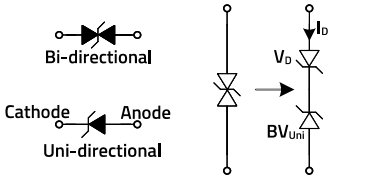
Figure 1: Electrical symbols for the uni- and bidirectional TVS diodes. Right figure: Functional equivalent of the bidirectional TVS diode.
The display on the right in Figure 1 shows how you can imagine a bidirectional TVS diode – as a circuit consisting of two TVS diodes connected in an “anti-serial” configuration. The typical voltage-current graphs of the diodes are displayed in Figure 2. The parameters from the graphs above and the WE datasheets have the following meanings:
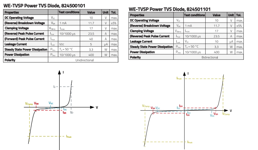
Figure 2: Graphs of unidirectional and bidirectional TVS diodes
DC operating voltage (VDC), channel operating voltage (VCh)
The maximum operating peak voltage must not exceed VDC. The TVS diode presents a high impedance to the protected circuit when the voltage across the diode is below this threshold value. Above this threshold, a high leakage current flows, which can lead to permanent failure of the TVS diode.
Reverse breakdown voltage (VBR)
This is the voltage threshold at which the TVS diode begins to conduct a defined current of 1 mA and is also referred to as the breakdown voltage. The value of VBR, according to the datasheet, should be above the maximum operating voltage of the circuit to be protected, so that the TVS diode remains in a reverse-biased state under normal operating conditions of the device.
Limiting voltage, clamping voltage (VClamp)
The overvoltage transient is limited to the value defined by VClamp, i.e., the maximum voltage that occurs in the protected circuit. The VClamp voltage is defined for a specific peak pulse current (IPeak).
Peak pulse current (IPeak)
This is the maximum surge current the TVS diode can withstand without damage. The peak pulse current is defined based on the transient waveform of the surge current, which is typically specified as 8/20 µs in most industrial applications, where 8 µs is the rise time (t1) to the peak value and 20 µs is the pulse duration until the current drops to 50% of the peak value (t2).
Leakage current (ILeak)
The leakage current is measured at VDC and is the residual current that flows in the reverse direction.
Power dissipation (PDISS)
The power dissipation PDISS indicates how much power the diode can absorb. A distinction is made between peak pulse power dissipation and the steady-state power dissipation.
Peak pulse power dissipation
The maximum peak power the TVS diode can dissipate during a transient event for a defined pulse waveform, in this case for the 10/1000 µs pulse (10 µs rise time, 1000 µs decay to half amplitude).
Steady-state power dissipation: The power the TVS diode can continuously absorb under normal operating conditions.
Ultra-low capacitance TVS diodes
There is a family of TVS diodes referred to as an ultra-low capacitance TVS diodes (or Super Speed Series, femtoF). They have a much lower capacitance than conventional TVS diodes, typically in the range of 0.1 to 0.5 pF, and are designed to protect high-speed data lines such as USB, HDMI, and Ethernet, as well as RF applications. The low capacitance is achieved by adding a forward-biased generalpurpose diode in series with the TVS diode, which is usually reverse biased. The functional structure is illustrated in Figure 3.
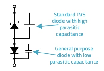
Figure 3: Functional structure of an ultra-low capacitance TVS diode.
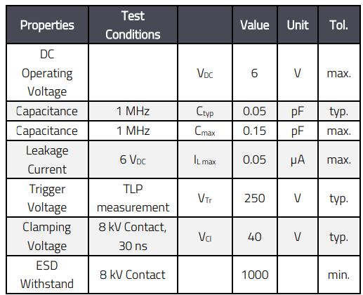
Table 1: Electrical characteristics of the “femtoF” TVS diode, 8231706A
2. TVS DIODES WITH “SNAPBACK” EFFECT
An ideal TVS diode completely blocks current, i.e., the current is zero when the input voltage is below the breakdown voltage. If the input voltage exceeds the breakdown voltage, the TVS diode ideally has a resistance close to zero, allowing the transient voltage to be effectively suppressed. A standard TVS diode clamps by beginning to conduct at a certain voltage and limiting the voltage drop across the diode. This diode exhibits a “non-ideal” behavior due to leakage currents and a finite low internal resistance (Figure 2).
A TVS diode can be realized by using a PN junction with a defined breakdown voltage. If a transient input voltage exceeds the breakdown voltage, current flows through the TVS diode to provide protection against transient voltages. However, the TVS type with a PN junction has no minority carriers and therefore exhibits poor clamping characteristics due to its high internal resistance. In semiconductor technology, there are alternative TVS implementations with bipolar NPN/PNP junctions in which a bipolar transistor provides the clamping property triggered by an avalanche effect. The base of the transistor is flooded with minority carriers, allowing the bipolar TVS to achieve a clamping voltage at a lower and constant level, as the avalanche current is increased by the transistor’s bipolar gain from its base.
This type of “TVS diode” is based on the internal structure of MOSFET components and is significantly more complex than the circuit diagram of the TVS diode (Figure 1) suggests.
Every NMOS-FET contains a parasitic bipolar junction transistor (BJT) resulting from the configuration of the doped material. In normal operation of an NMOS component, the parasitic BJT does not take effect. As displayed in Figure 4, the BJT has the source as the emitter and the drain as the collector, and the underlying p-substrate can serve as the base of the BJT given the right conditions.
At this point, the “impact ionization” must be explained to further understand the function: A mobile electron or hole (positive charge carrier) moves under the influence of an electric field. In a weak electric field, it moves without changing the system. In a strong electric field, however, such as in a component with high voltage across its terminals, the mobile charge carrier encounters energetically bound charge carriers, which can then be liberated. These new charge carriers can, in turn, repeat the process, resulting in an avalanche current.
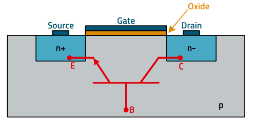
Figure 4: Parasitic bipolar junction transistor (BJT) in the NMOS FET.
When this avalanche current moves towards the base of the parasitic BJT, the base current can open the BJT and allow a large current to flow between the collector and emitter. The most interesting aspect of this is that after the component is opened, i.e., turned on, the high electric field that initiated the process is no longer necessary or even present to maintain the current. The conduction of current continues as the current increases, but at a much lower voltage between the emitter and collector. This phenomenon of triggering at a relatively high voltage and then falling back into conductivity at a lower voltage is known as snapback.
High-bandwidth data and signal buses require multi-channel TVS diode arrays for ESD protection. Figure 5, for example, shows the circuit diagram of a two-channel transient protection on the left, and the functional circuit diagram of the TVS diode array on the right.
Figure 6 shows the cross-sectional view of the core of the four-channel array in the upper part, and its functional equivalent circuit diagram in the lower part. The TVS array includes a variety of high-side and low-side steering diodes connected in series, with the high-side steering diodes connected to VCC and the low-side steering diodes connected to ground potential. In addition, these high-side and low-side steering diodes are connected in parallel to a Zener main diode, the TVS diode (also see Figure 5). The steering diodes are much smaller and have a lower junction capacitance.
A p-WELL is a region within an n-type semiconductor substrate that is doped with p-type impurities. This creates a localized region of p-type material within the n-type substrate.
An n-WELL is a region within a p-type semiconductor substrate that is doped with n-type impurities. This creates a localized region of n-type material within the p-type substrate.

Figure 5: Transient protection at a USB interface with a TVS diode array
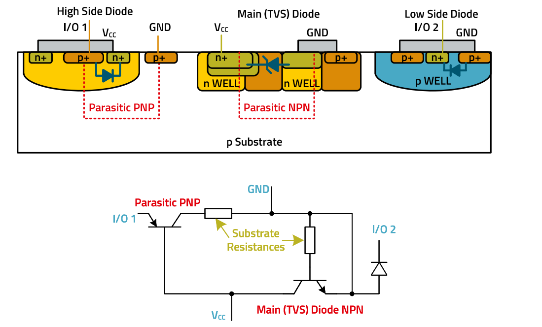
Figure 6: Cross-section of the core of a four-channel TVS diode array and its functional circuit diagram.
In practice, implementing the function as shown Figure 6 proves to be challenging. Contemporary technologies for manufacturing a TVS array face the technical difficulty that in a TVS array – in which multiple PN junction diodes are created in a semiconductor substrate through the application of a standard CMOS processing step – there are inherent parasitic PNP and NPN transistors. When a transient voltage occurs, the parasitic NPN or PNP transistors of this TVS array are turned on and “locked”, causing a sudden and strong voltage rebound, known as the snapback effect, as already explained with the bipolar transistor (Figure 4). This effect arises between the source-body diode of a PMOSFET or NMOSFET, and an N+ in P-substrate junction, where a parasitic siliconcontrolled rectifier (SCR) is formed as a parasitic component (Figure 7).
When the SCR is triggered, a strong current path is formed between the P+ region (anode, An) and the N+ region (cathode, Ca). This, in turn, leads to the clamping effect. Figure 8 shows the characteristic VI curves of different silicon components for comparison: conventional semiconductor diode, NPN bipolar junction transistor (BJT), and SCR circuit.
The normal diode (Figure 8, left) undergoes Zener or avalanche breakdown at a specific voltage, known as the breakdown voltage VBR. For diodes with a VBR below 5.5 V, the ‘Zener breakdown’ predominates, whereas for diodes with a VBR above 5.5 V, the avalanche breakdown (avalanche effect) predominates. Once the breakdown voltage is reached, the current increases sharply while the voltage remains relatively constant. There is no snapback effect. The diode can be damaged if the current is not limited. An NPNBJT (Figure 8, middle) also undergoes avalanche breakdown in the collector-emitter region when the reverse voltage becomes too high. During breakdown, the collector current increases sharply, and the snapback effect occurs, in which the voltage at the collector suddenly drops as the current continues to rise. This can lead to the destruction of the transistor if the current is not controlled. An SCR (Figure 8, right) has a more complex breakdown mechanism due to its four semiconductor layers (p-n-p-n). The breakdown occurs when the voltage across the anode-cathode path reaches a critical threshold and the holding current is exceeded. After breakdown, the SCR can go into a conducting state and remains conductive even if the applied voltage decreases, until the current falls below the holding current, i.e., this also demonstrates the typical snapback effect, as with the BJT transistor. Figure 9 shows graphs of uni- and bidirectional TVS diodes with the snapback effect. For effective ESD protection, the trigger voltage should not be so high that it damages the circuit to be protected. Additionally, the lower holding voltage Vhold should be above the normal operating voltage of the circuit, which is ensured if the maximum operating voltage does not exceed VDC or VCh. If the TVS diode is not correctly selected, there is a risk of ‘latch-up’. The main reason for this is that when a transient overvoltage is coupled into a USB interface, for example, the voltage of the external overvoltage (ESD) is greater than the TVS breakdown voltage, which causes the TVS diode to turn on. If the wrong type of TVS diode is used in the circuit to be protected, the lower holding voltage Vhold is lower than the normal operating voltage, and the TVS diode remains conductive even after the external interference has passed. In this case, the power supply is shorted, or the TVS diode may burn out, which, in the worst case leads to damage to the device. Similarly, at high temperatures, the SCR can be triggered by a high leakage current through the NP junction of the parasitic NPN BJT, which, in turn, leads to latch-up. The datasheet specifications should therefore be observed.
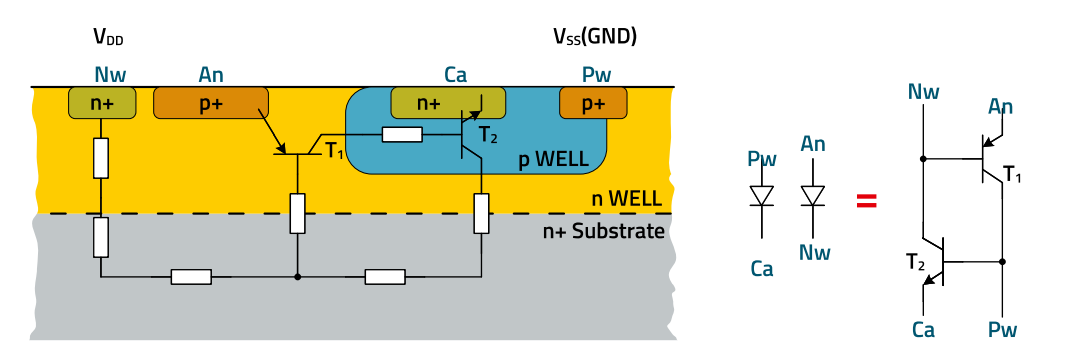
Figure 7: Schematic structure and equivalent symbols of an SCR in a CMOS process. The SCR is formed by the cross-coupled parasitic BJTs of the diodes.
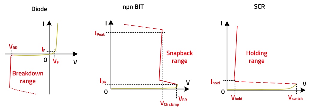
Figure 8: Comparison of the characteristic VI curves of different silicon components: conventional semiconductor diode, N-P-N bipolar junction transistor (BJT), and SCR circuit.
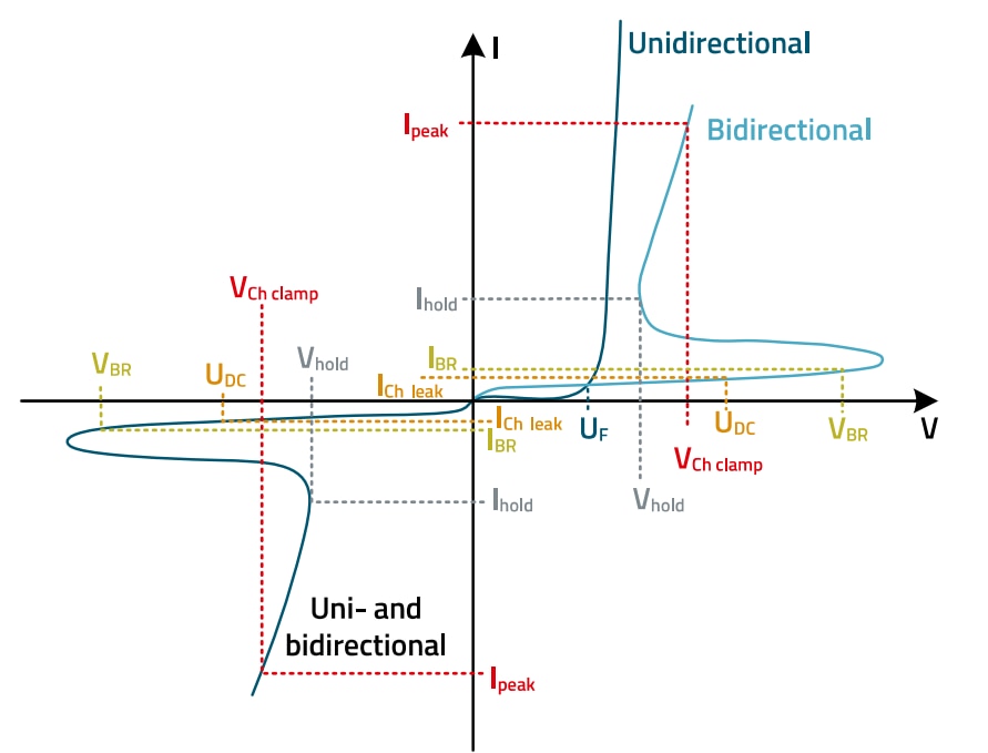
Figure 9: Characteristic VI curve of bidirectional TVS diodes with snapback effect.
3. TVS DIODE HYBRID FOR SIGNAL AND DATA LINES
A voltage-limiting component must provide protection against transient events without impairing the normal operation of the circuit. This can be a challenge, as the parameters often work against each other. A TVS diode for high-frequency signal interfaces should have a low capacitance to avoid signal distortion due to capacitive load. However, the ability of a component to absorb energy depends on the size of the junction. The larger the junction, the more energy it can absorb. The downside is that as the size of the junction increases, and the capacitance of the component also increases. As shown in the first section, a common method to reduce the effective capacitance is the use of a lowcapacitance diode circuit in conjunction with the TVS (Figure 3).
To protect multiple, symmetrical signal buses such as USB 3.1, multiple diode circuits are combined into an “array”. Figure 10 shows an example. The VI curve was measured using the Transmission Line Pulsing (TLP) method to obtain the necessary signal rise time for determining the clamping voltage VCH Clamp. It is a common measurement method specified in IEC 62615:2010 and has become established to demonstrate the behavior of components under ESD conditions. The method guarantees precise and repeatable measurement.
The capacitance of the TVS diode is practically “hidden” from the circuit by the conventional diodes. The diodes must withstand the transient current and require a reverse breakdown voltage that is higher than the breakdown voltage of the TVS diode.
Figure 10: Diode array with TVS diode for four channels, WE-TVS High Speed Series, 824015.
The resulting array is a component consisting of multiple functional regions. The integration and the resulting chassis ensure the required parameters for high-speed applications. For different applications, various IC groupings are available to achieve the required electrical parameters, making them easy to integrate into circuits. Typical schematic symbols are shown in Figure 11.
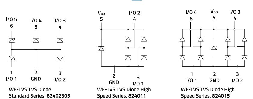
Figure 11: Different TVS diode arrays.
4. DC AND AC BEHAVIOR OF TVS DIODE ARRAYS
In the following section, various results from lab experiments are presented taking the TVS diode array WE-TVS 824015 to illustrate the function of this type of component, its applications, and its limitations. Figure 12 shows the schematic diagram and the electrical parameters of the array
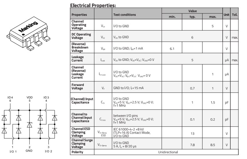
Figure 12: Schematic diagram and electrical parameters of the TVS diode array WE-TVS 824015.
4.1 Clamping behavior of the TVS diode
This section explains the necessary conditions for safe and controlled clamping behavior. It shows the snapback effect and describes the behavior of the component when used in a deficient PCB design. The experimental setup for data acquisition is a lab setup that can be reconstructed in a wellequipped lab. The data provided in the component datasheet was measured using a ‘transmission line pulse generator’, which offers high reproducibility and low error tolerance. To measure the clamping effect, the experimental lab setup displayed in Figure 13 was chosen. The measurement was taken using a 1.5 GHz active probe and a storage oscilloscope with a measurement bandwidth of 1 GHz to be in a position to display the fast processes
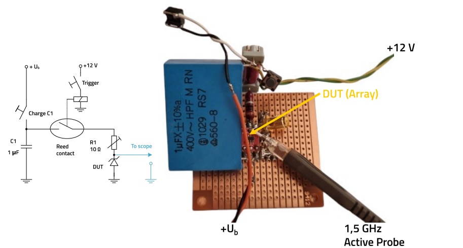
Figure 13: Setup for measuring the TVS diode clamping behavior.
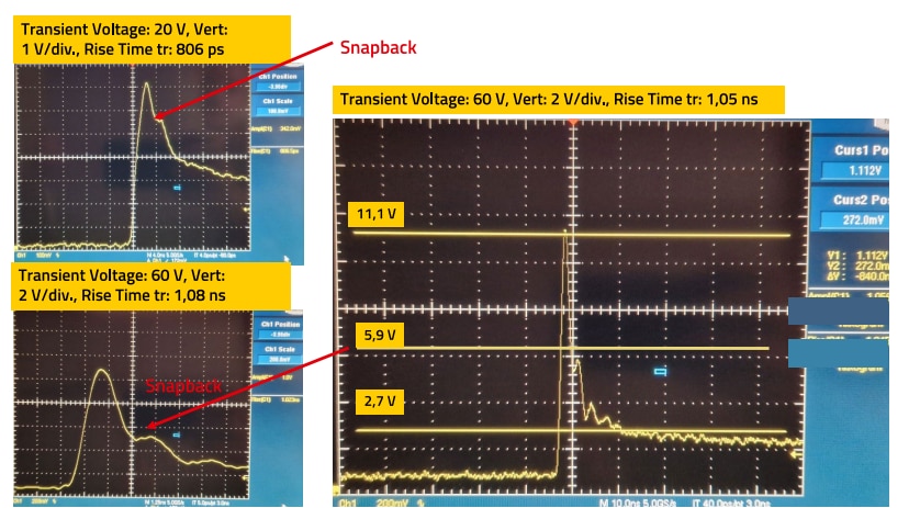
Figure 14: Clamping behavior of the TVS diode array
Besides the component-specific parameters, the clamping behavior depends very much on the setup. The main parameters here:
- Impedance and energy of the source, here the discharge capacitor C1
- Impedance of the lead from the energy source to the TVS diode, here defined by R1
- Impedance of the ground (GND), impedance between the energy source and the TVS diode
To carry out a defined discharge without switch bounce, a gasfilled reed relay was used in the setup, which was controlled by an auxiliary voltage. The measurement results are shown in the following images in Figure 14.
Upon applying a 60 V transient, the TVS diode used begins to conduct at approximately 11.2 V. The clamping voltage is observed as a ramp at around 5.9 V. The voltage in the circuit then gradually decreases as the capacitor voltage is disconnected by the relay. (Figure 13).
In Figure 15, the behavior of a conventional TVS diode is compared to the TVS diode of the array. The difference is clear: the conventional diode clamps without the snapback effect at around 8 V, while the TVS diode only begins to conduct at 7.7 V and then limits to approx. 5.8 V. Here there is no observable voltage decay because the capacitor remains connected.
In the theory section, it was described that the TVS diode itself is a complex structure of transistors, which causes the clamping effect through a mutual locking mechanism. This dynamic process includes a transition region of the VI curve, in which the slope of the characteristic curve and thus the resistance is negative. The snapback effect occurs when the voltage across the TVS diode drops to a lower value after breakdown, while the current continues to rise (Figure 9).
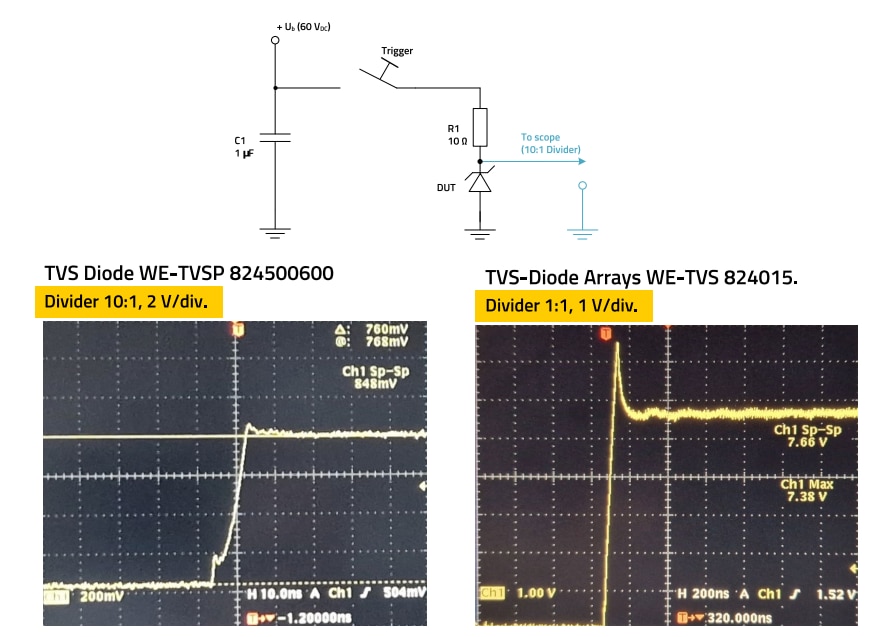
Figure 15: Clamping behavior of a conventional TVS diode, WE-TVSP 824500600, compared with the TVS element of the 824015 array.
This means that in a certain range of the VI curve, an increase in current leads to a decrease in voltage, which is referred to as negative differential resistance. This suggests that oscillatory behavior may occur in the transition region, which can be rendered visible and possibly usable in circuit design. To achieve this, it is necessary to pay more attention to the slope in the rise of voltage to be clamped, and here, in particular, the range around the breakdown voltage. A setup is chosen for this purpose that allows the current through the diode to be adjusted with a series resistor. The test setup and measurement results are displayed in Figure 16.
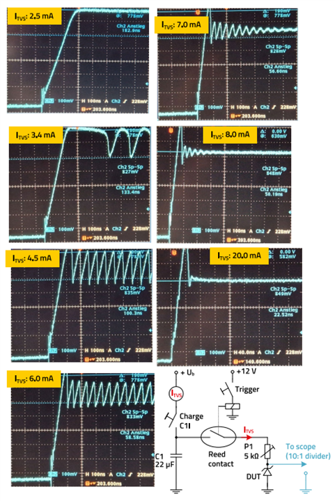
Figure 16: Test setup and behavior of the TVS element, displayed in the time domain.
At a low clamping current of 2.5 mA, the element shows clamping behavior without the snapback effect. The voltage is limited to 7.8 V. Starting from 3.4 mA, the component begins to oscillate, reaching its maximum amplitude at around 4.5 mA and decaying with increasing current to around 8.0 mA. The snapback effect is observed from 4.5 mA; at higher currents above 10 mA, the component shows the expected voltage limiting effect without oscillation and with the snapback effect, as displayed in the graph with a current of 20 mA. It should also be mentioned that the onset of oscillation depends not only on the clamping current but also on the load, i.e., the impedance of the oscillating element. Figure 17 shows the oscillation in both the frequency and time domains. A series resistor of 3.3 kΩ was used in the circuit for these measurements. The frequency range of the fundamental oscillation lies between 1.5 and 12 MHz.
The oscillatory behavior starts at a current of approx. 2 mA; at 15 mA, the signal amplitude is significantly smaller, and above 20 mA the oscillation stops. Certainly, you could repurpose the array and use it as an oscillator. But what does this behavior of the component mean for its intended function as a voltage-limiting component? Under normal conditions, this low current range up to 20 mA is exceeded within a few nanoseconds when a transient interference signal occurs. However, if the rise time of the interference signal is short, the component may be stimulated into temporary oscillation. It can also become critical if there are longer-lasting interference spikes on a useful signal whose level is just above the breakdown voltage of the TVS element. This case is displayed in Figure 18. The breakdown voltage of the TVS diode would be set too low for this application.
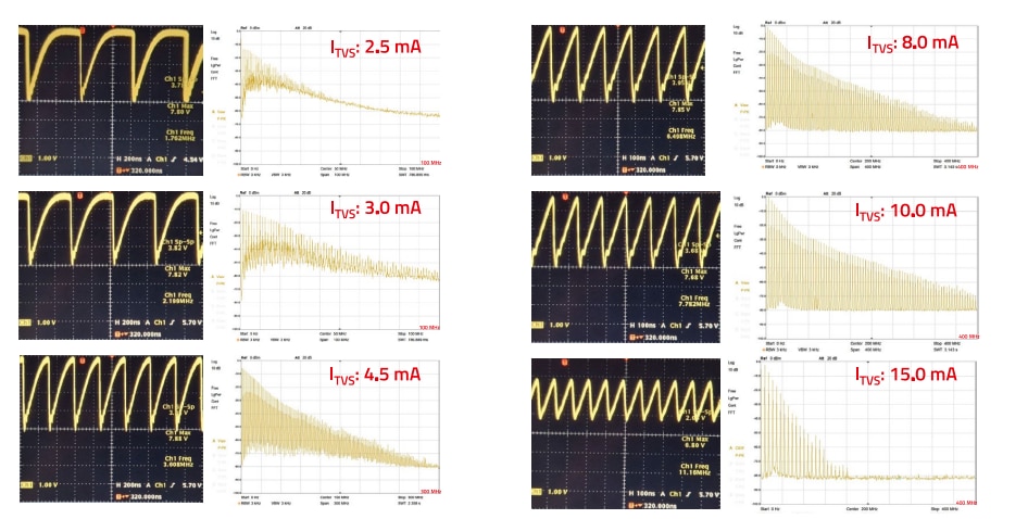
Figure 17: Oscillation of the TVS element as a function of the current ITVS.
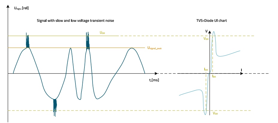
Figure 18: Interference signal on the useful signal with only a small amplitude.
4.2 Signal behavior of the TVS diode array
The main use of TVS diode arrays is for protecting signal interfaces. When using these arrays, the signal properties should not be impaired if at all possible. Both the amplitude and frequency properties are important here. The frequency properties are mainly related to the system impedance and the parasitic capacitance of the array. The amplitude properties are therefore considered in more detail below, as they do not directly result from the functional circuit diagram, which is shown in various displays in Figure 19.
From the display of the steering diodes as a bridge rectifier shown in Figure 19 on the lower right, it can be seen that the maximum signal level between I/O 1 and I/O 2 depends on the bias voltage between VDD and GND. To determine the threshold value, the setup shown in Figure 20 was chosen. The signal voltage between I/O 1 and I/O 2 is not grounded, i.e., it is configured as a symmetrical signal and therefore has no ground reference to the power supply. Practical examples included USB, HDMI and Ethernet signals. The capacitor C1 decouples any DC voltage that may occur to protect the signal generator. R1 decouples the signal between the signal generator and the array for detecting distortion. The electrolytic capacitor C2 is the equivalent of the filter and back-up capacitor in real applications and short-circuits AC signals. R2 serves as the load, i.e., for discharging the voltage when the voltage at the lab power supply is reduced.
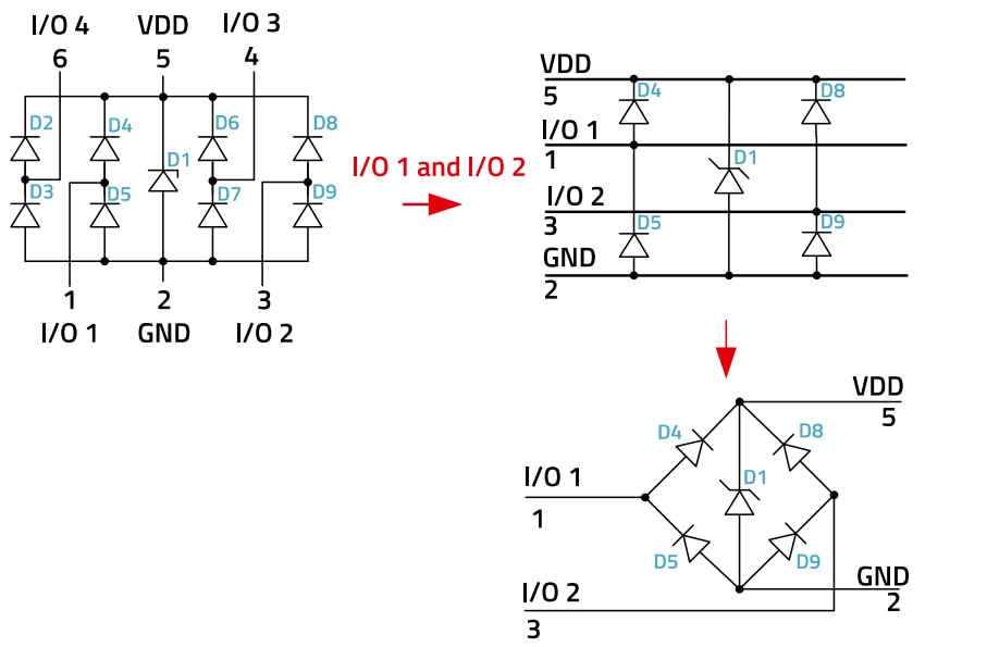
Figure 19: Different displays of two channels of the TVS diode array.
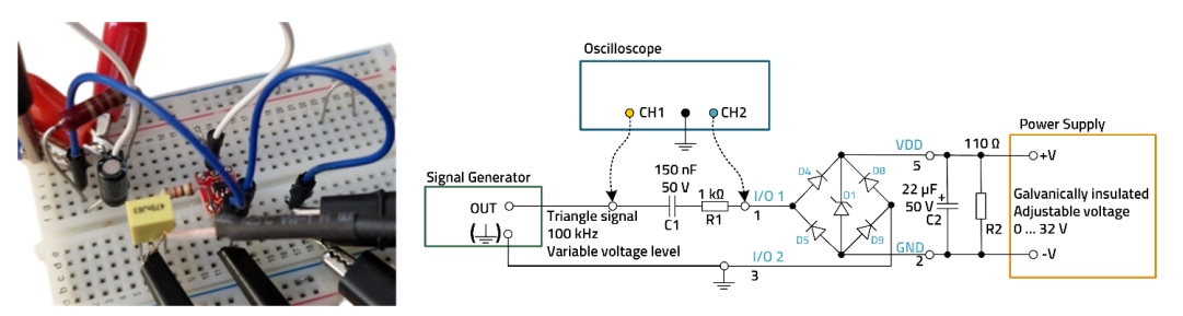
Figure 20: Setup for measuring the maximum input amplitude VPP as a function of the bias voltage VDD.
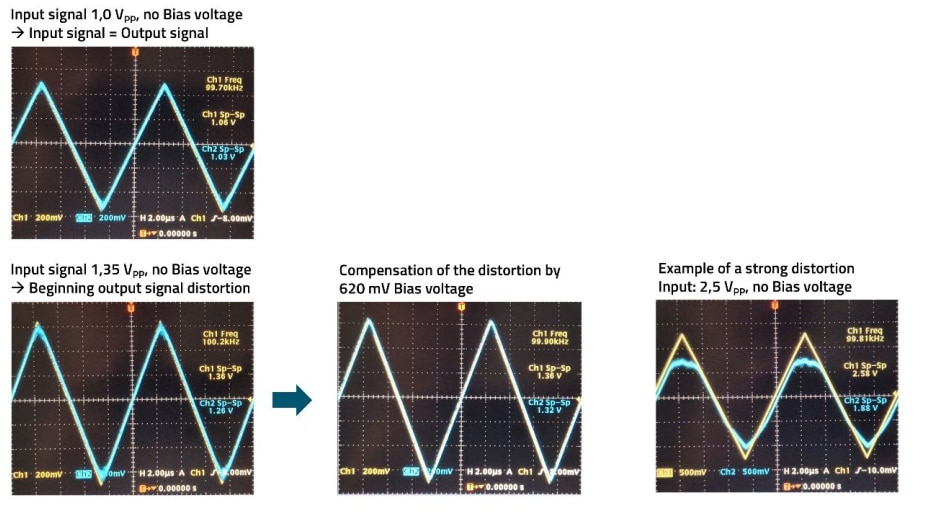
Figure 21: Examples of signal distortion as a function of the bias voltage.
By comparing the signals of the two channels CH1 and CH2, it is easy to determine the necessary bias voltage VDD to avoid distortion by the array. It is shown that the dependence is not linear. Figure 21 displays examples of signal distortion as a function of the bias voltage.
It can be seen that the distortion range begins at approx. 1.3 VPP signal amplitude. Amplitudes above this level require a bias voltage for the diodes between VDD and GND (DC bias). The asymmetry in the last trace in Figure 21 results from the onset of forward current IF of the TVS diode. The graph of the signal voltage as a function of the bias voltage is displayed in Figure 22.
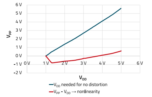
Figure 22: Graph of the signal voltage as a function of the bias voltage.
The blue curve shows the bias voltage VDD required to achieve a distortion-free signal voltage Vpp. The progression is not linear, as can be seen from the red difference curve (VPP – VDD). In the signal level range just above 1.35 VPP, only a low bias voltage is required to compensate for the distortion. As the signal voltage increases, the bias voltage must also increase, whereby the differential difference does not remain constant.
The non-linearity arises from the diode characteristic curve of the “steering diodes”, and the diode characteristic curve is shown in Figure 23. It is apparent that the forward voltage range begins at approx. 0.8 V, i.e., according to Figure 20, for two steering diodes, a signal voltage of 1.6 VPP will certainly affect the signal if the VDD, according to the blue curve in Figure 22, is smaller than VPP.
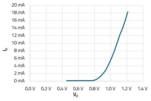
Figure 23: Diode characteristic curve of the “steering diodes".
4.1 TVS diode array variations
The following section compares different arrays to demonstrate their function and potential applications. The lab setup with the associated circuit diagram is shown in Figure 24.
A 100 kHz triangular signal was input for the measurement, whose level is gradually increased. If the level was limited on one of the three channels, the DC voltage VCCa was increased accordingly to apply an offset to the steering diodes. The following is an overview of the results with a brief explanation of the graphs in the “Remarks” column and a more detailed clarification at the end of the figure.

Figure 24: Lab setup with the associated circuit diagram for comparing different TVS diode arrays.

Figure 25: Comparison of the signal behavior of different TVS diode arrays, according to Figure 24, left part.
The 824015 array limits the signal beyond the forward voltage of the steering diode, i.e., from about 0.7 V, corresponding to 2 x 0.7 VSS (2nd trace in Figure 25). A bias voltage gives the diode a voltage offset in the reverse direction, so the signal can be increased up to the offset voltage plus the forward voltage (3rd trace in Figure 25). In the bottom trace in Figure 25, the signal level for the 824015 array (yellow curve) exceeds the forward voltage of the steering diodes, so without bias, the level is limited to about 1.4 VPP. In contrast, for the 82400102 array (blue curve), the blocking diode to VDD acts such that the signal is not limited in its positive half-cycle. The negative halfcycle, however, is limited by GND. For the 82402305 array (purple curve), the Zener breakdown voltage is not exceeded for the positive half-cycle and the negative half-cycle is limited to VF via the connection to GND.
4.2 Practical guidance
The following measurements show the behavior of the two TVS diode arrays 824021 and 824022 (Figure 24, right part). The “transient voltage” in the setup was 100 V, the discharge was through a pre-charged 1.5 µF capacitor. The power supply leads to the arrays were intentionally kept long. The measurement result in Figure 26 shows the typical snapback effect, and the measurement also confirms the approx. 1 V lower clamping voltage of the bidirectional TVS diode in the 824022 array. A resonant decay of the voltage is observed due to the parasitic inductances of the power supply. Furthermore, the breakdown voltages VBR of the two diodes are relatively high, ranging between 26 and 31 V.
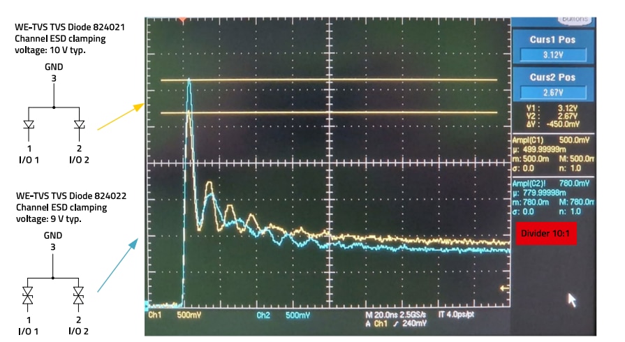
Figure 26: Clamping behavior of the two arrays according to Figure 24, right part
Here it is clear how important an RF-compatible design is, i.e., an RF-compatible layout in practice. The TVS diode must be integrated with low impedance in the current path in order to be effective. The following measurement was carried out under significantly better conditions. Figure 27 shows the test setup for the 824021 array with the corresponding measurement result. The breakdown voltage is now only 18.7 V and the clamping voltage is 7.4 V. Finally, a practical application is shown. Figure 28 displays the circuit diagram of a USB 3.1 interface. The signal lines are protected against transient overvoltage by TVS diode arrays. The reference ground is the chassis, because the overvoltage, such as an electrostatic discharge, has the chassis or the earth as its ground reference.
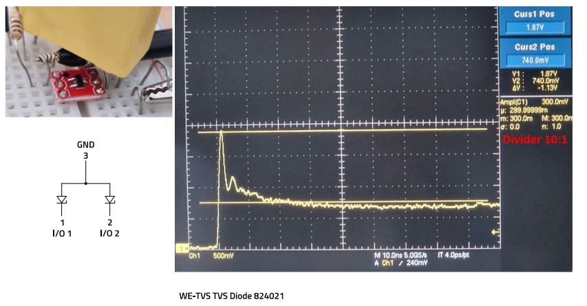
Figure 27: Setup and results for measuring the breakdown and clamping voltage.
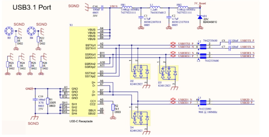
Figure 28: Circuit diagram of a USB 3.1 interface.
Figure 29 shows the layout around the TVS diode arrays. The arrays are routed in the signal path, with the ground connection made directly to the SGND area to ensure the shortest possible ground connection.
SGND is the ground of the package, as displayed in Figure 29, left. The ground of the USB controller, which follows the inductors L2, L3, and L5, is “GND”. The connection between SGND and GND is made through the components R21 – R26 in Figure 28, top left and R1, C19, C44 in Figure 29. For a detailed description, please refer to the reference designs RD016 and RD022, which can be downloaded from the website.
4.3 Other applications and circuit examples
The following section provides an overview of the various applications of TVS diodes and TVS diode arrays. For each application category, different circuits are presented to facilitate transfer to other applications.
4.5.1 Transient protection for DC inputs
In the following circuits, TVS diodes are used to limit overvoltage, whether caused by transient interference in terms of EMC or by “signal overvoltage”.

Figure 29: Layout of the USB 3.1 interface around the TVS diodes.
4.5.1.1 Protection of rectifier diodes
The circuit in Figure 30 shows part of a power supply with a transformer and rectifier.
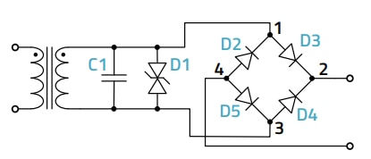
Figure 30: TVS diode for protecting rectifier diodes.
The bidirectional TVS diode D1 protects the rectifier diodes D2-D4 from transient differential overvoltage, i.e., commonmode transients are not limited here. The capacitor C1 attenuates low-energy high-frequency transient overvoltage, while the TVS diode limits the typical burst and surge transients. The circuit is useful where Schottky rectifier diodes with low forward voltage are used, as they generally also have a low maximum reverse voltage. C1 should typically be in the range 5 - 10 nF, and the clamping voltage of the TVS diode must, of course, be lower than the maximum reverse voltage of the Schottky diodes.
4.5.1.2 Protection at the DC input of a device
The following circuit in Figure 31 shows a filter with transient protection for a DC input to power a device.
On the primary side of the common-mode inductor, the TVS diodes D22, D29, and the filter capacitors C106, C107 are connected to the chassis ground (SGND). The 824520241 TVS diodes have a breakdown voltage of 28.1 V and limit transient overvoltage that occurs in common mode. The capacitors, together with the current-compensated choke L13 and capacitors C108 and C109, form a π-filter for each current path (X4/1 and X4/2). The bidirectional TVS diode D1 limits differential overvoltage, which can be caused by the switching processes of inductive loads located in the nearby same circuit. The clamping voltage of the diode must be below the maximum permissible input voltage of the downstream DCDC controller. On the secondary side of inductor L13, at the transition between C109 / C2, the electronics ground and the chassis ground are connected. Figure 31 also shows the layout of the filter. It is clearly apparent that the TVS diodes are placed right at the interface input and are “looped” into the current path, i.e., directly into the trace lead, to prevent a current bypass. For more information, please refer to reference design RD041, which can be downloaded from the WE website.
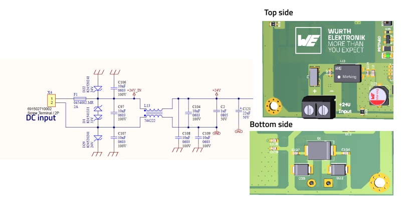
Figure 31: Protection at the DC input of a device.
4.5.1.3 Protection at the measuring probe input of a device
The circuit in Figure 32 is an instrumentation amplifier as part of a measuring device. IN- and IN+ are the differential inputs for measuring the voltage in a system. The voltage to be measured passes through the Wheatstone bridge to the non-inverting inputs of the OP amps. The bidirectional TVS diodes limit transient voltages against the primary ground (S_GND, chassis), which here also serves as the reference ground for common-mode interference.
The diodes clamp at 10.3 V and have a parasitic capacitance of typically > 1 nF, which, along with the bridge resistors, forms a low-pass filter at the input of the OP amps. If high differential overvoltages are expected, an additional bidirectional TVS diode can be installed in place of C1; J4 is then replaced with a wire bridge.
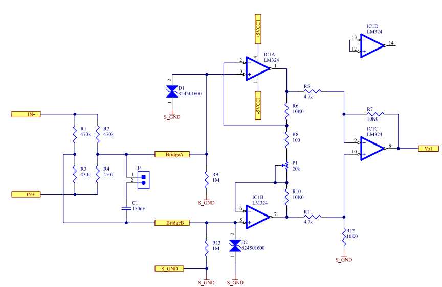
Figure 32: Protection at the measuring probe input of a device.
4.5.2 Protection of an HDMI interface
The HDMI interface is now an important standard for many electronic devices. To reduce the risk of ESD damage to the HDMI connectors, manufacturers not only conduct tests on the plug or chassis, but also perform direct pin discharge to improve ESD robustness. To minimize signal distortion, the transmission channels D0, D1, D2, and CLK must be impedance-matched, and the TVS diodes for ESD protection must have a low parasitic capacitance.
The traces between the TVS diode and the line to be protected, as well as between the diode and the ground plane, must also be as short as possible to minimize the influence of inductance on the clamping voltage, because the parasitic inductance of the trace adds an additional voltage drop to the clamping voltage of the ESD protection device. Figure 33 shows the part of an HDMI interface with ESD protection.
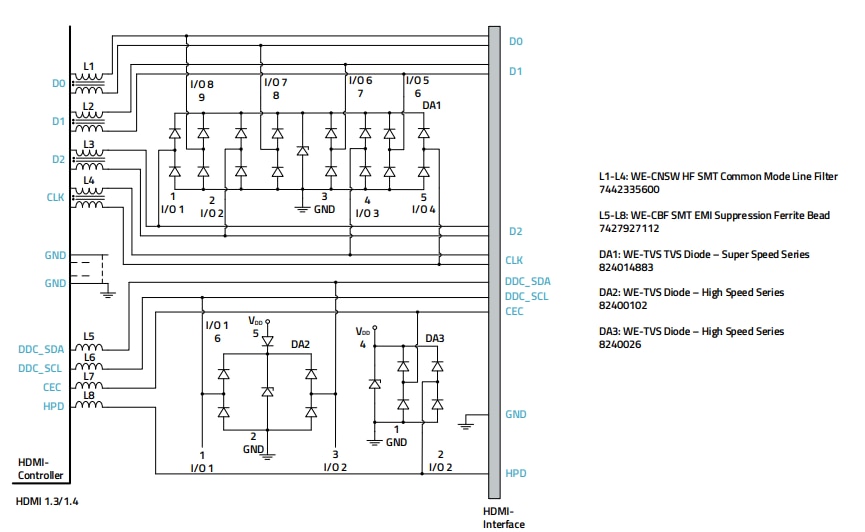
Figure 33: Section of the circuit diagram of an HDMI interface with ESD protection.
Why is a TVS array (DA2) with an additional diode used in the DDC_SDA and DDC_SCL lines? If the HDMI sink is connected to the HDMI source (see Figure 34), a leakage current path can form through the protection diode of the TVS diode array at the source when the source is turned off (Figure 34, right), while the sink is in the boot state. This issue has been addressed in the TVS diode array 82400102 and effectively prevented by incorporating a backflow protection diode, as displayed in Figure 34.
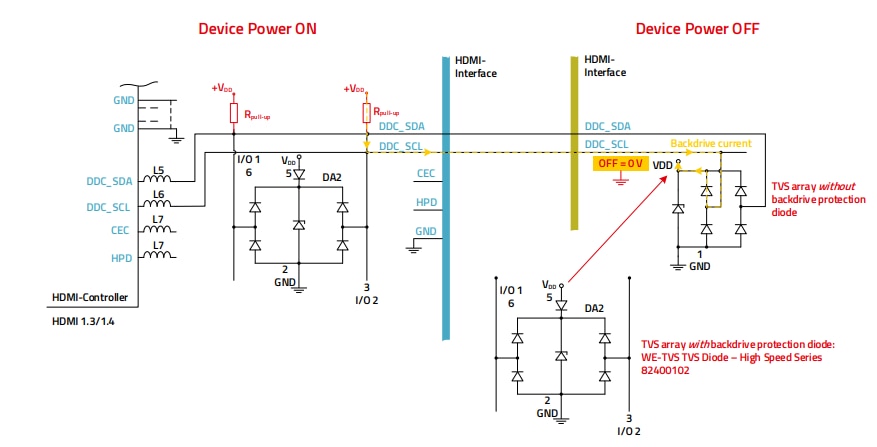
Figure 34: Excerpt from an HDMI interface system, display of the backflow current issue.
5. FINAL REMARKS
This extensive Application Note explains in detail how TVS diodes are constructed, how they function, and the pros and cons of these components. The electrical parameters of these complex components must be taken into account in the application to ensure the desired protection against transient overvoltage is achieved. Furthermore, proper circuit design and layout are necessary to prevent parasitic effects from significantly impacting the function of the TVS diodes. Numerous examples show how the components can be used properly.
A APPENDIX
A.1 Literature
[1] Decreasing the Loading Effect of the TVS Diode Using a Transmission Line for RF and Microwave Applications, Emad Zia Khodadadian and Mojtaba Joodaki, LETTERS ON ELECTROMAGNETIC COMPATIBILITY PRACTICE AND APPLICATIONS, VOL. 3, NO. 1, MARCH 2021.
[2] How to select a Surge Diode, Texas Instruments, Application Report, SLVAE37–January 2019.
[3] Latch-up free vertical TVS Diode Array structure using trench isolation, United States Patent, Patent No.: US 7,880,223 B2, Date of Patent: Feb. 1, 2011.
[4] Latch-Up, Texas Instruments, White Paper SCAA124-April 2015.
[5] Electrostatic discharge protection, United States patent, Patent No.: US005416351A, Date of Patent: May 16, 1995.
[6] Transient suppressing device and method, United States patent, Patent No.: US 6,392,266 B1, Date of Patent: May 21, 2002.
[7] Transient voltage suppression device, United States patent, Patent No.: US 6,867,436 B1, Date of Patent: Mar. 15, 2005.
[8] Transient voltage suppressor without leakage current, United States patent, Patent No.: US 8,785,971 B2, Jul. 22, 2014.
[9] Compound semiconductor materials, silicon diode wavers, URL: https://www.powerwaywafer.com/de/silicon-diode-wafer.html
[10] Snapback behavior determines ESD protection effectiveness, Semi-Wiki, URL: https://semiwiki.com/eda/magwel/7189-snapback-behavior-determines-esd-protection-effectiveness/
[11] Embedded. Ninja, TVS-Diodes, URL: https://blog.mbedded.ninja/electronics/components/dio des/tvs-diodes/
[12] Referenzdesign Notes RD016, RD022, Würth Elektronik eiSos,URL: https://www.we-online.com/en/components/products/WE-LAN-RJ45
[13] Würth Elektronik eiSos, Reference design note REF041, Design of a Single Pair Ethernet System with Power over Data Lines, URL: https://www.we-online.com/en/components/products/WE-STST
[14] Würth Elektronik eiSos, Application design note ANS020, Digital Isolators, URL: https://www.we-online.com/en/components/products/di/digitalisolators-without-power
IMPORTANT NOTICE
The Application Note is based on our knowledge and experience of typical requirements concerning these areas. It serves as general guidance and should not be construed as a commitment for the suitability for customer applications by Würth Elektronik eiSos GmbH & Co. KG. The information in the Application Note is subject to change without notice. This document and parts thereof must not be reproduced or copied without written permission, and contents thereof must not be imparted to a third party nor be used for any unauthorized purpose. Würth Elektronik eiSos GmbH & Co. KG and its subsidiaries and affiliates (WE) are not liable for application assistance of any kind. Customers may use WE’s assistance and product recommendations for their applications and design. The responsibility for the applicability and use of WE Products in a particular customer design is always solely within the authority of the customer. Due to this fact it is up to the customer to evaluate and investigate, where appropriate, and decide whether the device with the specific product characteristics described in the product specification is valid and suitable for the respective customer application or not. The technical specifications are stated in the current data sheet of the products. Therefore the customers shall use the data sheets and are cautioned to verify that data sheets are current. The current data sheets can be downloaded at www.we-online.com. Customers shall strictly observe any product-specific notes, cautions and warnings. WE reserves the right to make corrections, modifications, enhancements, improvements, and other changes to its products and services. WE DOES NOT WARRANT OR REPRESENT THAT ANY LICENSE, EITHER EXPRESS OR IMPLIED, IS GRANTED UNDER ANY PATENT RIGHT, COPYRIGHT, MASK WORK RIGHT, OR OTHER INTELLECTUAL PROPERTY RIGHT RELATING TO ANY COMBINATION, MACHINE, OR PROCESS IN WHICH WE PRODUCTS OR SERVICES ARE USED. INFORMATION PUBLISHED BY WE REGARDING THIRD-PARTY PRODUCTS OR SERVICES DOES NOT CONSTITUTE A LICENSE FROM WE TO USE SUCH PRODUCTS OR SERVICES OR A WARRANTY OR ENDORSEMENT THEREOF. WE products are not authorized for use in safety-critical applications, or where a failure of the product is reasonably expected to cause severe personal injury or death. Moreover, WE products are neither designed nor intended for use in areas such as military, aerospace, aviation, nuclear control, submarine, transportation (automotive control, train control, ship control), transportation signal, disaster prevention, medical, public information network etc. Customers shall inform WE about the intent of such usage before design-in stage. In certain customer applications requiring a very high level of safety and in which the malfunction or failure of an electronic component could endanger human life or health, customers must ensure that they have all necessary expertise in the safety and regulatory ramifications of their applications. Customers acknowledge and agree that they are solely responsible for all legal, regulatory and safety-related requirements concerning their products and any use of WE products in such safety-critical applications, notwithstanding any applicationsrelated information or support that may be provided by WE. CUSTOMERS SHALL INDEMNIFY WE AGAINST ANY DAMAGES ARISING OUT OF THE USE OF WE PRODUCTS IN SUCH SAFETYCRITICAL APPLICATION.
DIRECT LINK
ANP143 | TVS diodes: basics, function and their applications
USEFUL LINKS:
Application Notes : https://we-online.com/en/support/knowledge/application-notes
Services: https://we-online.com/en/products/components/service
Contact : https://we-online.com/en/support/contact
CONTACT INFORMATION
Würth Elektronik eiSos GmbH & Co. KG
Max-Eyth-Str. 1, 74638 Waldenburg, Germany
Tel.: +49 (0) 7942 / 945 – 0
Email: appnotes@we-online.de
