


Application Note
Transient protection SIP-3
ANS023 by Timur Uludag
1. INTRODUCTION AND THEORETICAL BACKGROUND
Transient over voltages often occur in industrial environments due to an extensive electrical infrastructure. In order to develop an efficient filter to limit transient over voltages, many influencing parameters must be considered. Today, many industrial applications run on logic input voltage levels such as 5 VDC or lower, as shown in Figure 1. The power distribution system used to power such applications often run on a DC bus voltage of 24 VDC. Switching DC/DC converters are commonly chosen to handle the conversion of the higher DC bus voltage down to the lower logic voltage level.
Figure 1 shows the basic electrical structure of an industry plant. The separated parts of the applications are supplied through a DC bus. On site, every separated electrical load is connected via a sub distribution with 24 V. Non-isolated power modules are implemented to provide the operating voltage of all subsystems.
1.1 Origin of Transients
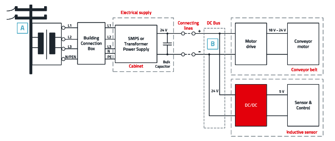
Figure 1: Industrial environments typically use a DC bus to power the individual elements of a plant
Transient over voltages can be defined as short-term deviations from a nominal voltage value, which exceeds the permissible tolerance range of the nominal voltage in an electrical system. The effects of the transient over voltages are mostly destructive. First and foremost, there is more than one possible cause for a transient over voltage on the DC bus that leads to an abrupt rise. The origin of the over voltage can be a lightning strike (Figure 1, Part A), in which case we speak of a surge, or it can be generated in the system itself (Figure 1, Part B). Classically, the output of switched mode power supplies (SMPS ,DIN Rail power supply) specify surge voltage on output according to the EN 61000-4-5 between a positive and negative value ranging from 500 V to 1 kV. Since the output of the DIN rail power supply is connected directly to the input of the DC/DC converter, it needs to have the same test severity levels. Improper and nonexistent surge/transient protection leads to malfunctioning due to electrical damage to the DC/DC converter, leading to higher system downtimes and costs. For a correct calculation, we must use a standardized transient pulse as defined in the IEC 61000-4-5 standard as a so-called surge.
1.2 Filter Concept
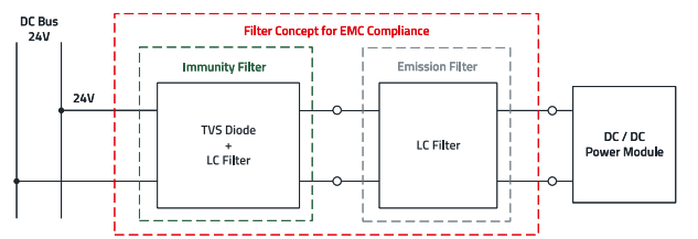
Figure 2: Filter concept for EMC compliance of MagI³C power modules with immunity and emission filter
Figure 2 shows the entire immunity filter concept (green), which includes two stages of filtering. One stage to clamp the high transient overvoltage during a surge event, which can be achieved with transient suppressor components such as unidirectional TVS diodes. For the second stage, a passive LC filter is recommended, which attenuates the voltages that exceed the maximum operating voltage of the DC/DC converter. For optimization purpose the two filter stages could be merged into one filter stage that includes both, the immunity and the emission filter. This application note targets the step-by-step approach with two separate filter stages as this is the easiest.
2. IMMUNITY FILTER DESIGN LIMITS
In many cases, two different values are specified in the data sheet in the chapters "ABSOLUTE MAXIMUM RATINGS" and "OPERATING CONDITIONS". The value in the "ABSOLUTE MAXIMUM RATINGS" one is the absolute maximum input voltage VPM_MAX, which, if exceeded, will result in permanent damage to the power module The other is the maximum operating voltage, which corresponds to the maximum input voltage specified by the manufacturer for which the power module is properly used. To protect against transient overvoltages, it is recommended that the immunity filter is designed so that the absolute input voltage of the power module never exceeds the absolute maximum input voltage VPM_MAX, even during transient overvoltage events. For further calculations the 173010535 SIP-3 power module with an absolute maximum input voltage of VPM_MAX = 44 V is used as an example [1].
2.1 Immunity Filter Design
In this article, the use of a unidirectional TVS-Diode is considered as a protection element for the power module input. Unidirectional operational behavior means that the V-I characteristics are nearly the same as that of a Zener diode. Consequently, the diode is normally used in reverse direction. Exceeding the component’s specific breakdown voltage causes the TVS diode to enter into a conductive state. The clamping voltage level is then determined by the current flowing through the component. The following numerical example provides a simplified, hands-on guide for establishing a filter. The filter estimation enables a quick refinement cycle when conducting real application tests. To make a proper design based on a TVS diode for a transient protection of the power module, the following parameters are required.
- VDC: supply voltage for the power module
- VBR: voltage where 1 mA of current is flowing through the TVS diode
- IPEAK: max. peak current flowing through the TVS diode @ VCLAMP_MAX
- PDISS: maximum dissipated power for the TVS diode
- VCLAMP_MAX: voltage where the diode carries the Ipeak
2.2 First Immunity Filter Stage
Determination of VDC The maximum occurring DC bus voltage is decisive for the interference immunity of VDC, not the nominal value. With a 24 V bus, the voltage range of 19.2 to 30 V is specified in industrial environments. Consequently, the maximum value for VDC is 30 V.
The selection of the TVS diode for the next steps of calculation is based on the available parts in the product portfolio of Würth Elektronik. The TVS diode 824550301 [2].is selected for the further calculation as it comes closest to the requirements.
Determination of VBR
VBR is defined as the voltage at which 1 mA of current is flowing through the TVS diode. This value, in this case 35.05 V, is not exactly fixed, as it is a PN junction whose voltage can vary slightly due to tolerances and operating conditions. The tolerance is given in the datasheet as ±5%. That leads to a VBR from 33.33 V to 36.80 V. In this region, the diode starts its conduction with a current of 1 mA. However, it is also necessary to know the value at which the transient voltage should be clamped. This is represented by the parameter VCLAMP_MAX.
Determination of VCLAMP_MAX
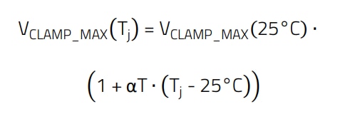
This value can be found in the datasheet as well. For the chosen diode, the voltage is 48.4 V based on a peak current of IPEAK of 31 A, representing a 10/1000 µs pulse. So far, the calculations have assumed an ideal laboratory environment with a controlled ambient temperature of 25°C. However, the reality looks different. From experience an ambient temperature around 55°C is common for electronic devices such as a TVS diode. Therefore, the calculation needs to be modified with a temperature factor. Mainly VCLAMP_MAX and the peak pulse power are strongly dependent on the temperature. Equation (1) shows the temperature effect to VCLAMP_MAX.
 (1)
(1)
In the “standby case”, in which almost no current flows through the TVS diode apart from the leakage current of 1 µA, the junction temperature (Tj) is almost the same as the ambient temperature. Assuming a temperature coefficient αT for this type of TVS of 9.9 × 10⁻⁴ 1/°C, this results in a maximum VCLAMP of 49.84 V at 55°C. This value will be now the starting point for the dimensioning of the second stage of the immunity filter.
2.3 Second Immunity Filter Stage
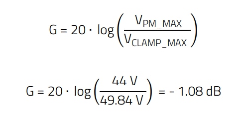
The question now is how to estimate the right filter attenuation and how to get the best filter component values. Starting with the attenuation, the minimum filter attenuation can be calculated with Equation (2).
 (2)
(2)
Instead of the symbol A (attenuation) the symbol G (gain) is used. A negative gain means an attenuation.
Equation (2) considers the resulting clamping voltage level VCLAMP_MAX of the TVS diode during the surge event and the maximum operating voltage level VPM_MAX of the chosen converter. The task is to design the filter according to Figure 3, where a LC filter circuit needs to be added to the TVS diode.
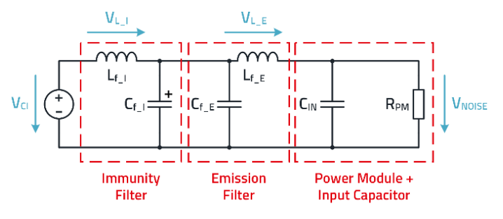
Figure 3: Equivalent circuit for second stage immunity filter calculation.
The designer, allowing for the calculation of a corresponding filter capacitor, can select the inductor value. The reason for this is that the filter inductor is in series with the application, and therefore its resistance (RDC) causes unwanted losses.
Therefore, the inductor with the smallest possible RDC value concerning the nominal maximum output current of the DC/DC converter should be selected. A WE-PD2 (744776112) with an inductance of 12 µH, an RDC of 336 mΩ and a rated current of 2.72 A was selected for this example filter design.The DC input resistance of the power module can be determined with the given input and output voltage, the output current as well as the efficiency during operation.
Putting these parameters together, Equation (3) for the converter input resistance can be established.
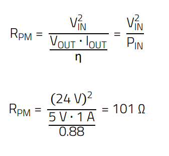 (3)
(3)
Figure 3 shows the equivalent circuit where the TVS diode is represented as a simplified voltage source. The remaining portion of the circuit diagram for the EMC model consists of two LC filters for immunity (surge protection) and emission (EMI attenuation), the input capacitor of the DC/DC converter and the input resistance of the regulator.
As this is an indoor application and therefore an indirect surge caused by the overvoltage occurs, the following assumptions and calculations are based on an 8/20 µs pulse as defined in the IEC 61000-4-5 standard. For further simplification, it is possible to omit Cf_E and Lf_E since this filter is designed to suppress disturbances at the switching frequency of the power module (Figure 4).
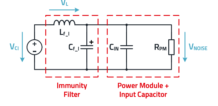
Figure 4: Simplified equivalent circuit for second stage immunity filter calculation.
The power module switches typically at 520 kHz. Looking at the frequency spectrum of the surge impulse, one can determine that the highest value of the noise voltage occurs at a frequency of f = 1 kHz. That’s why the over voltage is based on 1 kHz.
To get the attenuation G of the filter, it is necessary to compare the output voltage to the input voltage of the system (Equation (4)).
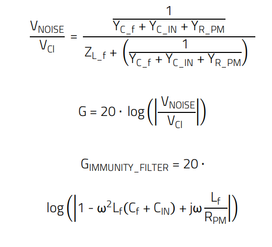 (4)
(4)
With the previously calculated DC input resistance RPM in of the converter, Equation (5) can be used to establish the necessary capacitor value:
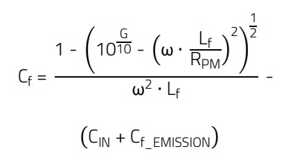 (5)
(5)
Here Lf represents the immunity filter inductor, RPM the DC input resistance of the converter, CIN the input capacitor and Cf_EMISSION the EMI filter capacitor of an input PI filter structure. The values can be found in the datasheet of the power module 173010535. Assuming the use of a 12 µH inductor, the calculation result for the filter capacitor is Cf = 218 µF. Checking the standard values for capacitors, a value of 220 µF (860010775018) is chosen as it is larger than the calculated value. A value less than the calculated capacitance would not provide sufficient attenuation of the filter. The final filter selected components are as follows: TVS diode = 824550301, Lf_I = 744776112, Cf_I = 860010775018.
The influence of the temperature on the VCLAMP_MAX and thus on the value of the filter capacitor, is shown in Table 1.
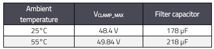
Table 1: Temperature influence overview
The capacitor values have been calculated, but real capacitors are subject to relatively high tolerances. The actual capacitance value can vary by up to ±20 %. If the temperature dependence of the VCLAMP_MAX is not fully accounted for, a capacitor with too low a capacitance value may be selected.
2.4 Transient Protection and EMI
In order to develop an efficient filter to limit transient over voltages, many influencing parameters must be considered. This is particularly important for an application in an industrial environment, since transient over voltages often occur here due to the extensive electrical infrastructure. The filter with transient protection enables efficient protection of the DC/DC converter module under consideration and simultaneously enables damping of high-frequency emissions.
Figure 5 shows the complete EMC concept for the immunity and emission filter. The values for the components used, are shown in Table 2.
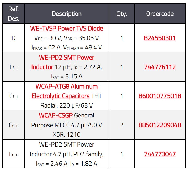
Table 2: BOM for immunity and emission filter.
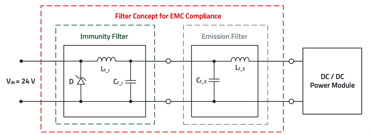
Figure 5: EMC compliance filter concept of MagI³C power modules with immunity and emission filter.
A APPENDIX
A.1 Literature
[1] Würth Elektronik data sheets for SIP-3 power modules: https://www.we-online.com/MAGIC-FDSM
[2] Würth Elektronik data sheets for TVS diodes: https://www.we-online.com/WE-TVSP
IMPORTANT NOTICE
The Application Note is based on our knowledge and experience of typical requirements concerning these areas. It serves as general guidance and should not be construed as a commitment for the suitability for customer applications by Würth Elektronik eiSos GmbH & Co. KG. The information in the Application Note is subject to change without notice. This document and parts thereof must not be reproduced or copied without written permission, and contents thereof must not be imparted to a third party nor be used for any unauthorized purpose. Würth Elektronik eiSos GmbH & Co. KG and its subsidiaries and affiliates (WE) are not liable for application assistance of any kind. Customers may use WE’s assistance and product recommendations for their applications and design. The responsibility for the applicability and use of WE Products in a particular customer design is always solely within the authority of the customer. Due to this fact it is up to the customer to evaluate and investigate, where appropriate, and decide whether the device with the specific product characteristics described in the product specification is valid and suitable for the respective customer application or not. The technical specifications are stated in the current data sheet of the products. Therefore the customers shall use the data sheets and are cautioned to verify that data sheets are current. The current data sheets can be downloaded at www.we-online.com. Customers shall strictly observe any product-specific notes, cautions and warnings. WE reserves the right to make corrections, modifications, enhancements, improvements, and other changes to its products and services. WE DOES NOT WARRANT OR REPRESENT THAT ANY LICENSE, EITHER EXPRESS OR IMPLIED, IS GRANTED UNDER ANY PATENT RIGHT, COPYRIGHT, MASK WORK RIGHT, OR OTHER INTELLECTUAL PROPERTY RIGHT RELATING TO ANY COMBINATION, MACHINE, OR PROCESS IN WHICH WE PRODUCTS OR SERVICES ARE USED. INFORMATION PUBLISHED BY WE REGARDING THIRD-PARTY PRODUCTS OR SERVICES DOES NOT CONSTITUTE A LICENSE FROM WE TO USE SUCH PRODUCTS OR SERVICES OR A WARRANTY OR ENDORSEMENT THEREOF. WE products are not authorized for use in safety-critical applications, or where a failure of the product is reasonably expected to cause severe personal injury or death. Moreover, WE products are neither designed nor intended for use in areas such as military, aerospace, aviation, nuclear control, submarine, transportation (automotive control, train control, ship control), transportation signal, disaster prevention, medical, public information network etc. Customers shall inform WE about the intent of such usage before design-in stage. In certain customer applications requiring a very high level of safety and in which the malfunction or failure of an electronic component could endanger human life or health, customers must ensure that they have all necessary expertise in the safety and regulatory ramifications of their applications. Customers acknowledge and agree that they are solely responsible for all legal, regulatory and safety-related requirements concerning their products and any use of WE products in such safety-critical applications, notwithstanding any applicationsrelated information or support that may be provided by WE. CUSTOMERS SHALL INDEMNIFY WE AGAINST ANY DAMAGES ARISING OUT OF THE USE OF WE PRODUCTS IN SUCH SAFETYCRITICAL APPLICATION.
DIRECT LINK
ANS023 | Transient protection SIP-3
USEFUL LINKS:
Application Notes : https://we-online.com/en/support/knowledge/application-notes
Services: https://we-online.com/en/products/components/service
Contact : https://we-online.com/en/support/contact
CONTACT INFORMATION
Würth Elektronik eiSos GmbH & Co. KG
Max-Eyth-Str. 1, 74638 Waldenburg, Germany
Tel.: +49 (0) 7942 / 945 – 0
Email: appnotes@we-online.de