Application Note
Digital isolators
ANS020 by Timur Uludag, Dr.-Eng. Heinz Zenkner
1. INTRODUCTION
The electrotechnical infrastructure has become very complex in recent years, whether in the industrial environment or in building technology. The decentralized recording of physical parameters is "state of the art" and high-performance microcontrollers facilitate the processing of data. However, recording the data from the object is often a challenge and wireless transmission of the data is frequently not possible. The data must be recorded from the object in such a way that the probe does not influence the quantity being measured as much as possible, otherwise measurement errors will occur. This requires electrical decoupling, which must be realized in the circuitry. Furthermore, the wired transmission of the data must be potential-free and symmetrical so that the transmission is not disturbed by electromagnetic coupling and ground loops. In this application, the use of microcontrollers was deliberately avoided in order to demonstrate that a highperformance, interference-free design can be realized with little effort using analog circuit technology. The design is divided into two circuits, a transmitter and a receiver. The transducer can record a DC voltage of ±30 Vmax with a fluctuation period of one second. The current consumption has been kept low. With a power supply of +15 V, it is <85 mA for the transmitter and <25 mA for the receiver. Both the transmitter and the receiver are galvanically isolated, at the transmitter between the measurement data acquisition and the signal transmission path and at the receiver between the signal transmission path and the data output. Special DC-DC power modules and digital isolators with galvanic isolation and particularly low parasitic coupling capacitance were used to realize this isolation in the circuitry. The signal is transmitted between the transmitter and receiver via a two-wire cable. Depending on the electromagnetic environmental influences, the distance can be several hundred meters.
2. BASIC CIRCUIT DESIGN OF A POTENTIALFREE VOLTAGE SENSOR
2.1 Basic Circuit Design-Transmitter
Figure 1 shows the block diagram of the transmitter. The circuit is divided into six blocks:
- Probe: Transducer with voltage divider and amplifier for measuring positive and negative polarity.
- Level shifter: Level shifter for the voltage-frequency converter.
- Voltage-to-frequency converter: Digital output signal, frequency dependent on the input voltage.
- Digital isolator: Galvanic isolation between measuring potential and interface.
- Interface buffer: Low-impedance line driver with balanced output.
- Power supply: DC/DC converter, galvanically isolated converters for the probe head section.
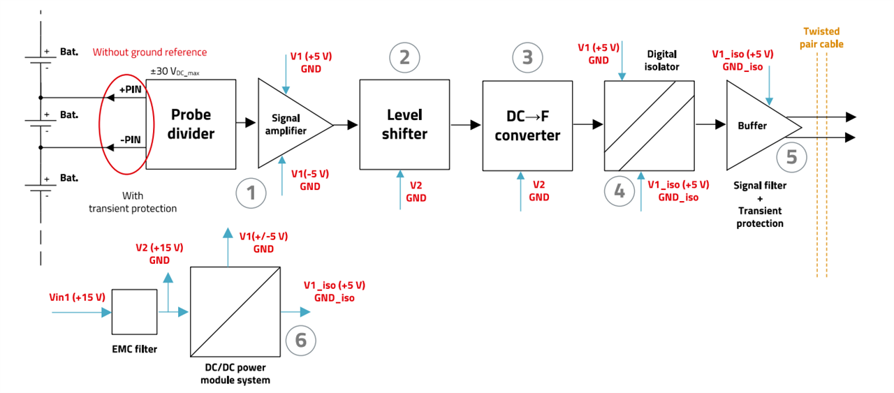
Figure 1: Block diagram of the transmitter for potential-free voltage measurements.
The block diagram shows that the design cannot be realized without EMC circuitry measures. To ensure functional reliability, transient protection and filters are provided both on the probe side and at the driver output; low-pass filters are also provided before and after the DC-DC power modules to effectively attenuate RF coupling.
2.2 Basic Circuit Design-Receiver
Figure 2 shows the receiver’s block diagram. The circuit is divided into five blocks:
- Input buffer: Signal pick-up, signal conditioning with balanced input. The link indicator shows whether there is a detectable connection to the transmitter.
- Digital isolator: Galvanic isolation between input signal and secondary signal processing / output interface. Additional galvanically isolated voltage for the input-side buffer.
- Frequency-to-voltage converter: Generates an output voltage from a digital signal. The voltage level depends on the frequency of the input signal.
- Interface buffer with polarity indicator: Level converter for the output signal. The output signal has a positive polarity, the polarity indicator shows the polarity of the input signal.
- Power supply: DC/DC converter for the secondary-side supply
Numerous EMC measures are also provided in the receiver section. The signal input coming from the twisted pair cable is equipped with transient protection and a common mode filter to effectively attenuate interference coming from the cable. The power supplies around the DC-DC converters are equipped with low-pass filters on both the input and output sides in order to significantly reduce both external electromagnetic interference and electromagnetic emissions from the DC-DC converters within the switching unit. This ensures a high signal-to-noise ratio and a high level of functional reliability.
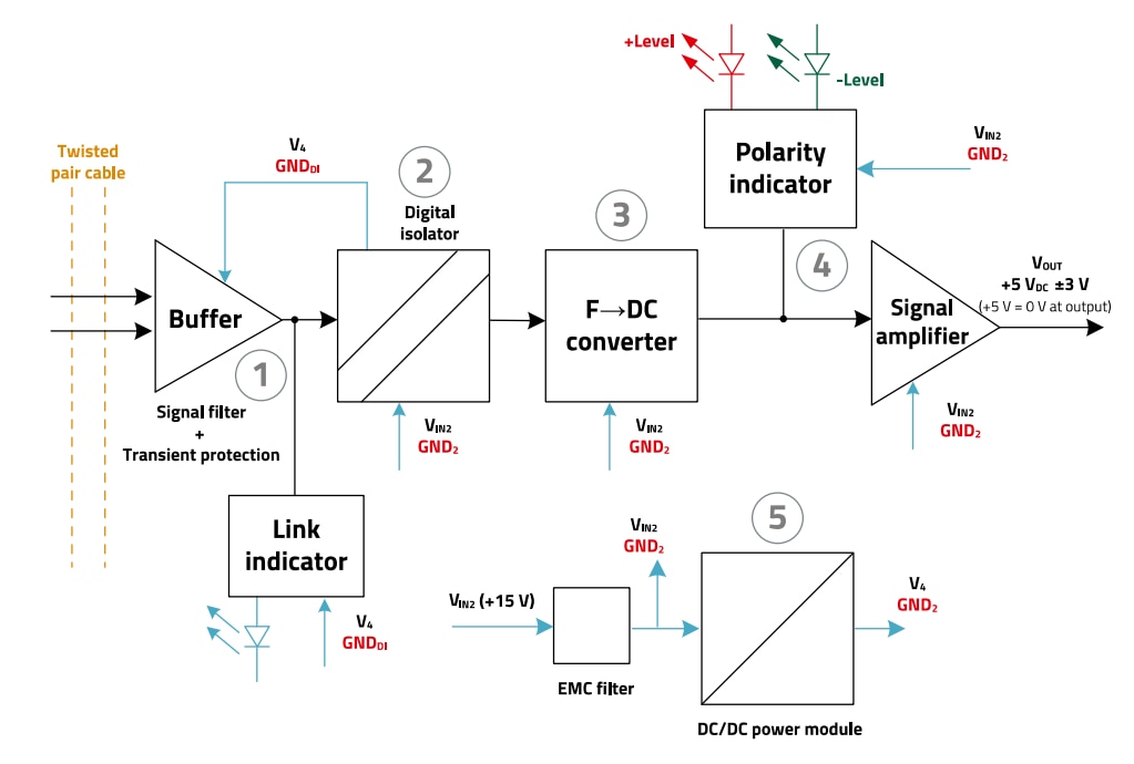
Figure 2: Block diagram of the receiver for potential-free voltage measurement.
3. KEY COMPONENT DIGITAL ISOLATOR AND ITS SPECIFIC PARAMETERS
Interference-free data communication and personal safety are two major challenges for electronics in this type of industrial environment. Strong electromagnetic fields, overvoltages, transient voltages and high EMC interference are the order of the day. If, for example, the communication line is laid unfavorably close to a control line of a frequency inverter, the pulses are capacitively coupled and the signals in the communication line oscillate with the pulse pattern of the frequency inverter. This interference can quickly reach a level where significant malfunctions occur and even the safety of people can be jeopardized.
If, for example, the temperature of a motor is measured with a thermocouple, voltages in the millivolt range are generated. If these voltages are now transmitted over a cable length of several meters to a central control unit that refers to a different earth potential, the measurement signal is distorted by the potential differences.
3.1 Functions of an Isolator
Clustering the described phenomena, the following four challenges emerge:
- A safety barrier between hazardous voltages and a user
- Separation of ground loops between spatial circuits
- Minimization of common-mode interference
- Interference-free data transmission
Figure 3 shows the situation of the data transmission system graphically. In order to meet the requirements of shielding dangerous voltages from the user and still guarantee interference-free data transmission, galvanic isolation must be used to separate the zones electrically, i.e. potentially from each other, so that they can work separately and thus without interference.
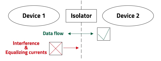
Figure 3: Basic concept of an isolated system to separate different potentials
The data flow runs via an isolator, but interference and potential equalization currents are held back by the galvanic insulation of the isolator.
3.2 Capacitive Digital Isolator
The digital isolator (block-diagram Figure 4) consists of an oscillator and a modulator on the primary side. On the secondary side are a demodulator and a buffer.
The primary-side components are galvanically separated from the secondary-side components by a capacitor structure with an isolation barrier made of SiO2.
Signal transmission through the isolation barrier is realized by a modulation method known as on/off keying. The oscillator integrated in the chip is used to modulate the Schmitttriggered input signal. The modulator generates a differential signal that is transmitted via the capacitively isolated lines.
The demodulator is located on the secondary side and is used to amplify, filter and reconstruct the input signal. The signal delay and distortion are minimal. Finally, the signal from the output of demodulator is passed through a buffer to the output; the buffer amplifies the signal to the required level.
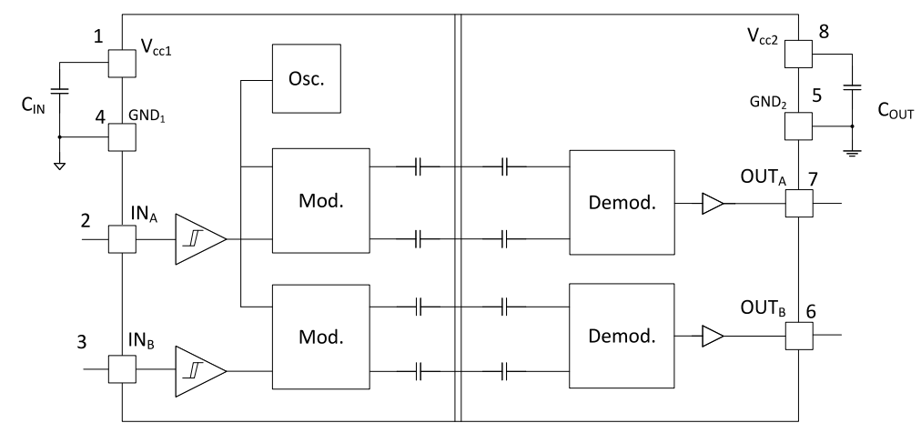
Figure 4: Block diagram of the CDIS 18012x15411x digital isolator.
Digital isolators are manufactured using standard CMOS technology and therefore use materials and processes that are well-known and tested. The capacitors of the transmitter side and the receiver side are deposited on a lead frame. The capacitors themselves, shown in gray in Figure 5, are formed between the two horizontal contacts, shown in red.
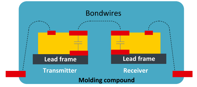
Figure 5: Basic structure of a capacitive digital isolator IC.
The dielectric material between the capacitor plates serves as a galvanic isolation barrier. The insulation thickness achieved by the process is in the range of a few tens of micrometers. In digital isolators, SiO2 is used as the insulating material in the capacitor because its much higher dielectric strength of 500 MV/m means that it requires considerably less space for the isolating gap. Other common insulation materials, such as polyimide, have a dielectric strength of only 300 MV/m. The two capacitors are electrically connected with a bonding wire so that the two capacitors are connected in series, as shown in the block diagram in Figure 4. To protect the entire structure, the die and leadframe are molded using a standard IC assembly process.
4. CIRCUIT DESIGN OF THE TRANSMITTER
The input for DC signal measurement is a Wheatstone bridge with four resistors, see Figure 6. This is followed by an optional capacitor with 150 nF (C1) for damping AC voltage components.
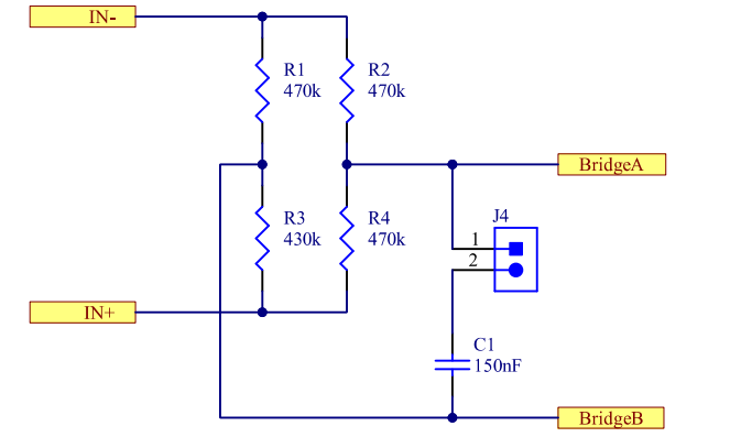
Figure 6: Wheatstone bridge as voltage divider at the input of the transmitter.
IC1A to IC1C in Figure 7 form an instrumentation amplifier whose amplification factor is set with P1. The input-side 1 MΩ-resistors (R9 & R13) are necessary for the stable operating point of the instrumentation amplifier and load the measuring signal with their resistance via the Wheatstone bridge. This results in an input impedance of approx. 450 kΩ.
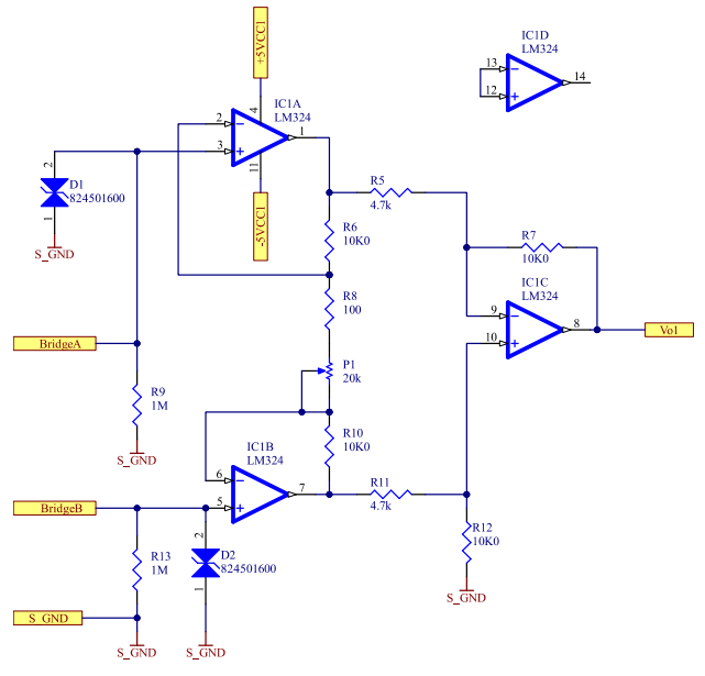
Figure 7: Discrete instrumentation amplifier for level amplification.
The bidirectional TVS diodes D1 and D2 clamp the input voltage at the instrumentation amplifier to a maximum of 10.3 V (Vclamp at Ipeak), but the current is limited by the voltage limitation via the Wheatstone bridge to such an extent that the clamping voltage is only slightly above the breakdown voltage of 7 V.
The maximum differential input voltage at one of the operational amplifiers is ±32 V, thus ensuring reliable transient protection. The circuit is designed so that a maximum voltage of ±30 V can be applied to the measurement input in order to control the instrumentation amplifier with a maximum of ±3.5 V at its output. The level should be equalized to ±3.0 V with P1.
As the signal can also have a negative polarity, it cannot be processed by the subsequent voltage-frequency converter. The level converter (level shifter) with IC2A and IC2B in Figure 8 converts the signal to a level range of 0 V to +10 V, whereby:
- -30 V at the DC measurement input -> 0 V at the level shifter output,
- 0 V at the DC measurement input -> +5 V at the level shifter output,
- +30 V at the DC measurement input -> +10 V at the level shifter output.
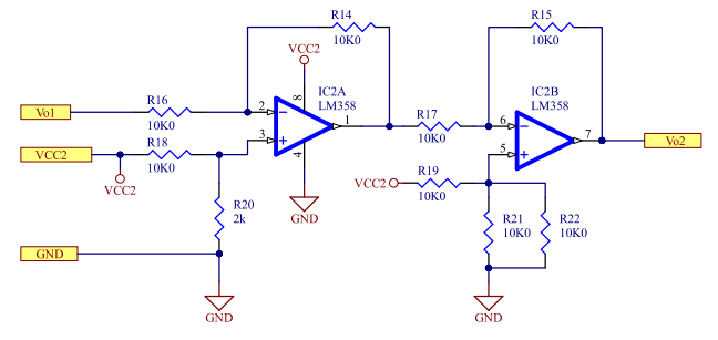
Figure 8: Level converter for level adjustment.
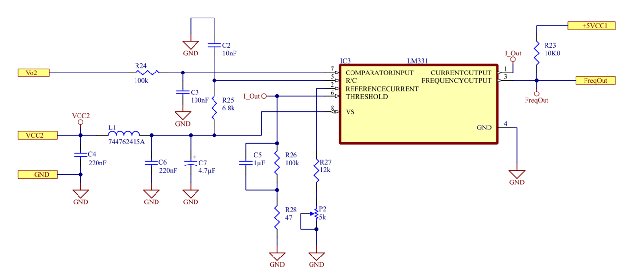
Figure 9: Voltage to frequency converter
The voltage-frequency converter (IC3) follows the level shifter converts the DC voltage into a square-wave signal (Figure 9). The wiring of the component results in the following relationship:
- -30 V at the DC measurement input -> 8 kHz at the output of the IC3,
- 0 V at the DC measurement input -> 5 kHz at the output of the IC3,
- +30 V at the DC measurement input -> 2 kHz at the output of the IC3.
The frequency can be fine-tuned using P2 on the IC3. The output voltage of the voltage-frequency converter depends on the supply voltage of the pull-up resistor (R23) on pin 3 of the component and is set to +5 V here.
The square-wave signal with a level of 0/+5 V passes from the voltage/frequency converter to the digital isolator (IC4).
The digital isolator selected here is the WPME-CDIS 18012015411L module. Only one channel of the 2-channel module is required here, the second channel is connected to earth on the input side so that no unwanted interference is coupled in.
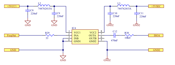
Figure 10: Digital isolator for galvanic isolation.
The digital isolator is supplied on both the primary and secondary sides via an electrically isolated power module (Figure 10). This ensures that the galvanic decoupling generated by the digital isolator is also ensured via the power supply on the primary and secondary sides. This results in a higher level of decoupling, even if the +15 V supply is not galvanically isolated on the primary side. This decoupling also leads to a reduction in the modulation signals generated by a digital isolator and thus allows a higher signal-to-noise ratio for the operational amplifiers. The signal reaches the buffer amplifier IC5 from the secondary side of the digital isolator (Figure 11).

Figure 11: Output stage
The op-amp provides a low-impedance differential output for the twisted-pair line to the receiver. The transmission signal is decoupled against high-frequency common mode interference via the choke L4, while the output is protected against transient overvoltage with the bidirectional TVS diodes D3 and D4. The stray inductance of L4 and the parasitic capacitance of D3 and D4 form a low-pass filter against common mode noise. The signal level at the output is:
- Input voltage: +30 V → transmitter output voltage, at 120 Ω impedance: 8.3 V at 8.5 kHz,
- Input voltage: -30 V → transmitter output voltage, at 120 Ω impedance: 6.4 V at 2.2 KHz.
The transmitter is supplied with a voltage of +15 V, the current consumption is <85 mA The +15 V input is HF-technically decoupled with a π-filter; depending on the application in the system, additional transient protection with a TVS diode may be necessary. A suitable component is the WE-TVS 824045810.
On the primary side of the digital isolator, the +5 V voltage can alternatively be tapped directly from the 5 V DC-DC Power Module (U1) FDSM series. If galvanic isolation is also required on the primary side, the 15 V supply should also be galvanically isolated.
The π-filter around the L5 choke attenuates RF interference and already has an insertion loss of over 64 dB at 1 MHz. Figure 13 shows the calculation result from REDEXPERT.

Figure 12: DC/DC primary side.
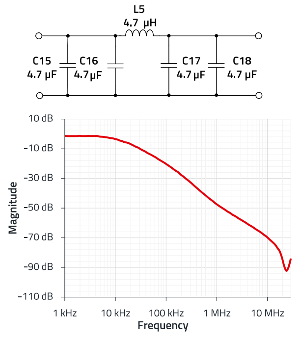
Figure 13: Insertion loss of the power supply filter simulated with REDEXPERT.
Both the voltage-frequency converter IC3 and the digital isolator WPME-CDIS (IC4) contain oscillators and switching stages that can cause harmonic interference. For this reason, each of these components has an additional low-pass filter connected to its supply connections.
The SMD ferrite choke WE-RFI 744762415A (L2 & L3) was used here, which allows broadband decoupling up to the 1 GHz range thanks to its high resonance frequency (maximum impedance at approx. 70 MHz). However, this requires a HF-compliant layout and the use of suitable capacitors (here: 220 nF / 50 V, WCAP-CSGP, 885012206125). The three galvanically isolated DC-DC power modules (shown in Figure 1) do not change the input voltage of +5 V, but "merely" isolate it. The decisive factor here is a parasitic capacitance of typically <10 pF, so that decoupling is achieved over the widest possible frequency range and common-mode interference is avoided as far as possible.
5. CIRCUIT DESIGN OF THE RECEIVER
The differential transmission signal reaches the receiver circuit via the cable section, depending on the length and therefore also the frequency-dependent attenuation. Two TVS diodes are placed directly at the input of the interface to attenuate transient overvoltages. The following capacitors block any DC voltage offset that may occur. The commonmode choke attenuates HF interference and forms a lowpass filter with the parasitic capacitances of the TVS diodes. The two diodes connected in an anti-parallel clamp the differential input voltage to approx. ±0.7 V, the rest drops across the 10 kΩ-resistors.
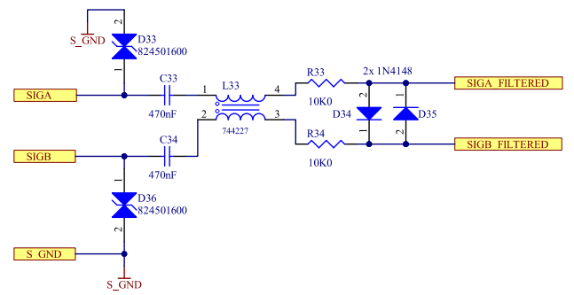
Figure 15: Signal amplifier of the receiver.
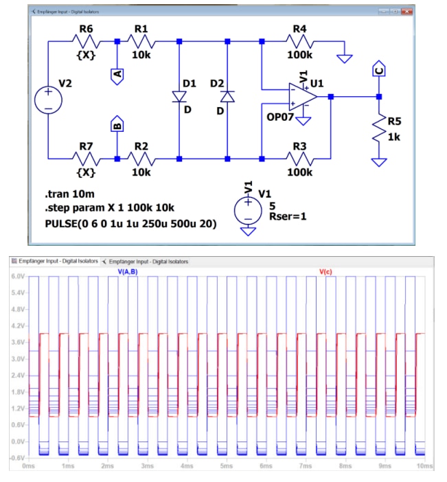
Figure 16: Simulation of the amplifier input stage with LT-Spice - circuit diagram.
The source voltage (V2) was assumed in the simulation to be 6 V at a frequency of 2 kHz, i.e. the input signal at a measurement voltage of -30 V. The cable resistance was varied from 2 Ω to 200 kΩ, the output voltage level remains constant at 3 V (0.9 Vlow to 3.9 Vhigh). In practice, it will not be possible to achieve the 200 kΩ cable resistance, as the impedance of the cable and electromagnetic environmental influences must be taken into account with increasing frequency, but distances of several hundred meters are feasible.
The amplitude-stabilized signal is sent from the operational amplifier IC33A to the:
- Digital Isolator IC34.
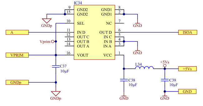
Figure 17: Digital isolator for galvanic isolation.
- “Link OK” amplifier or detector.
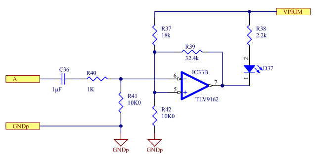
Figure 18: Link detector (LED on = link ok).
The "Link OK" amplifier IC33B (second OpAmp of the TLV9162) is connected as an inverting Schmitt trigger with offset and switches the blue LED to GNDp as soon as a signal is output at IC33A - this lights up the blue LED.
The digital isolator IC34 (WPME-CDIP 18024115401L) has an integrated galvanically isolated DC-DC converter, which is used to supply the input operational amplifier IC33A with voltage. This means that the module not only galvanically isolates the signal, but also the supply voltage between the input amplifier and further signal processing. As with the transmitter, the input-side power supply at the digital isolator is RF-technically decoupled via an LC filter. The digital signal is routed via a low-pass filter (L36 & C43) at PIN6 of the IC35 in order to reduce signal noise (Figure 19).
The dimensioning of the components depends on the signal bandwidth to be transmitted. Figure 19 shows the effect of the filter; in terms of circuit technology, this allows a lower phase noise to be achieved when converting the AC voltage signal into a DC voltage signal. The noise reduction is 200 mV, the cut-off frequency of the filter is approx. 800 kHz, so that any influence on the useful signal in this application can be virtually ruled out.
The signal passes from the filter of the digital isolator to the frequency-to-voltage converter IC35.
The trim potentiometer is used to fine-tune the output voltage and should be adjusted so that the output voltage is between 2.0 V and 8.0 V, depending on the measurement voltage at the transmitter, as described in section 4. The frequency converter is also provided with a filter for the +15 V supply voltage so that its switching signals do not couple into the power supply.
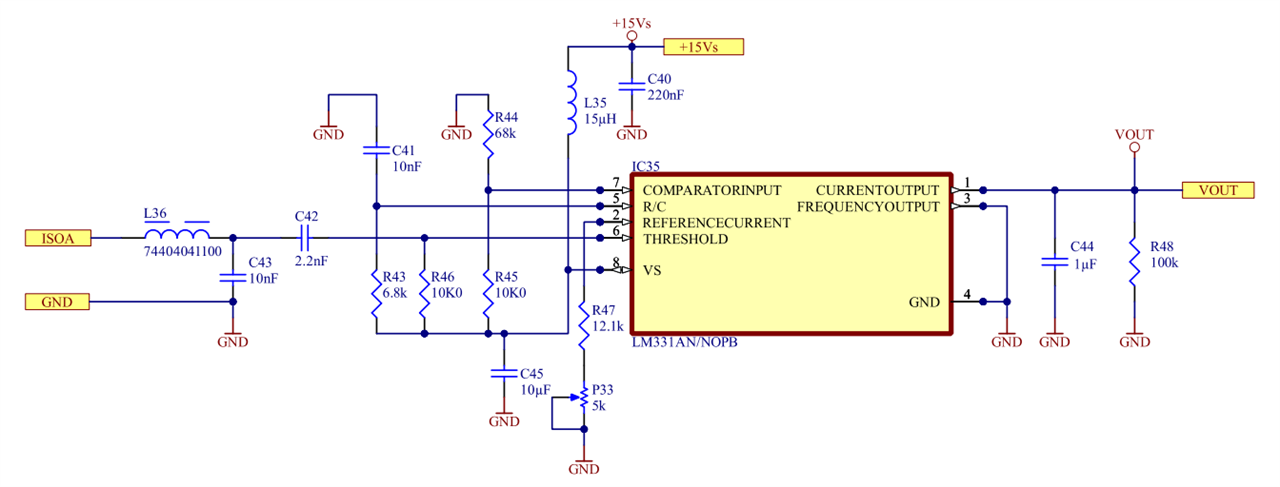
Figure 19: Frequency-voltage converter on the receiver.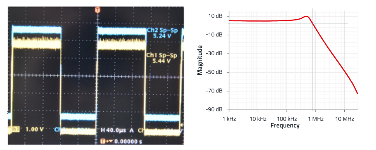
Figure 20: Filter for attenuating the signal noise for the F → U converter
The 1 µF/100 KΩ - RC element at the output of the converter smoothes the pulse-width modulated switching signals corresponding to the input frequency into a DC voltage. Depending on the combination of values, there are dependencies between response time, accuracy and residual ripple. For a more precise definition of the components, please refer to the manufacturer's datasheet.
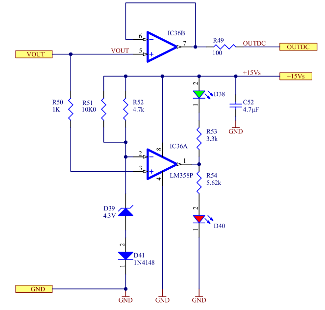
Figure 21: Polarity indicator for displaying the polarity of the measured voltage on the transmitter.
The polarity indicator (IC36A) at the output of the converter, shown in Figure 21, has the following function (Table 1):

Table 1: LED indicator on the receiver depending on the input voltage on the transmitter.
This allows the polarity of the measured signal to be detected. Furthermore, the signal from the frequency-to-voltage converter is also fed to an output driver, at the output of which the level transmitted and converted equivalent to the measured voltage is available. The signal can be divided again for further processing on an AD converter, and the polarity display can be fed to a microcontroller for polarity detection. The voltage supply of the receiver is +15 V at <25 mA. As the digital isolator provides the galvanically isolated power supply to the operational amplifier on the input side, no further power supply is required. As with the transmitter, the supply voltage is routed via a π-filter and fed directly to the frequency-voltage converter on the one hand and reduced to +5 V via the DC-DC regulator MagI³C-FDSM on the other in order to supply the remaining electronics.
6. TECHNICAL DATA
In summary, the application has the following performance data:
- Power supply transmitter: +15 V, <85 mA
- Power supply receiver: +15V, <25 mA
Figure 22 shows the relationship between the measured voltage and the voltage that is then displayed at the output.
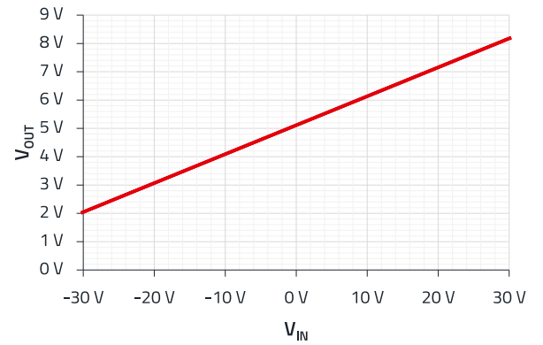
Figure 22: Diagram, input voltage over output voltage.
The transmission characteristic is almost linear over the entire input voltage range from -30 V to +30 V. The structure shown, consisting of a transmitter and a receiver board connected via a twisted pair cable, is therefore a suitable solution for galvanically isolated data acquisition and transmission.
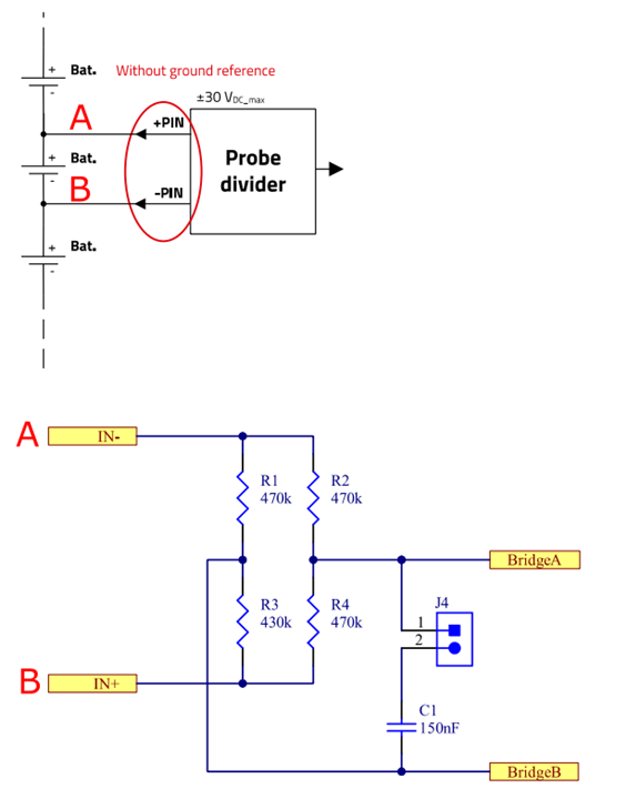
Figure 23: Measurement points A and B in Figure 1 and Figure 6 for Table 2
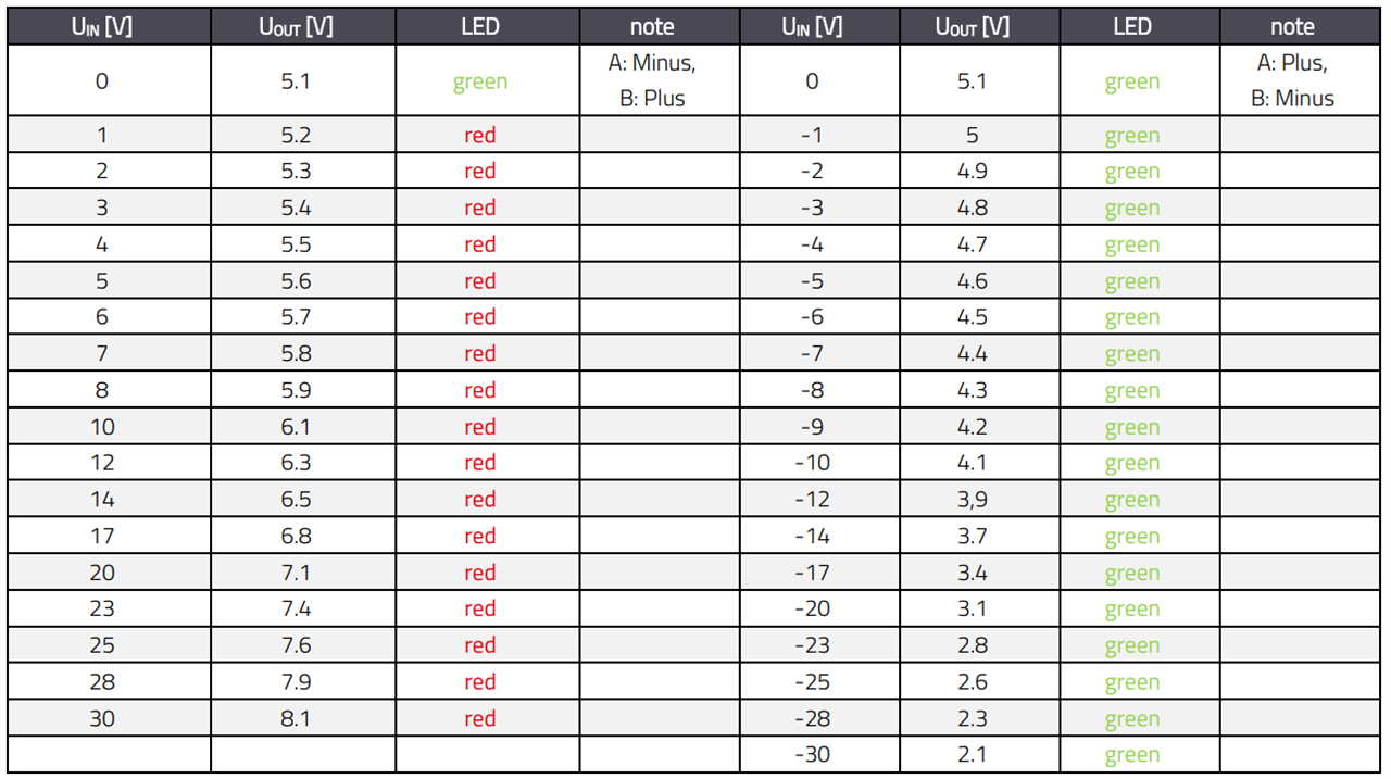
Table 2: Output voltage as a function of the input voltage.(see Figure 23 for reference)
A APPENDIX
A.1 References
[1] Maurizio Di Paolo Emilio, Power Electronics News: Reliable Galvanic Isolation, Simplified, URL: https://www.powerelectronicsnews.com/penebook-december-2023-delving-into-innovations-inpower-electronics-engineering/
[2] Würth Elektronik,18012015411L WPME-CDIS - Capacitive Digital Isolator Standard, URL: https://www.we-online.com/components/ products/datasheet/18012015411L.pdf
[3] Würth Elektronik,18024115401L WPME-CDIP - Capacitive Digital Isolator Powered, URL: https://www.we-online.com/components/ products/datasheet/18024115401L.pdf
[4] Texas Instruments, LM331 Precision Voltage-to-Frequency Converter With 1-HZ TO 100-KHZ Full Scale Frequency, SNOSBI2C, URL: https://www.ti.com/lit/ds/ symlink/lm231.pdf (June 1999–revised September 2015)
[5] Texas Instruments, TLV9162-Q, 1 Automotive, Dual, 16-V 11-MHZ Rail-to-Rail Input And Output Operational Amplifier, BOSAD7, URL: https://www.ti.com/lit/ ds/symlink/tlv9162-q1.pdf (April 2023)
[6] Texas Instruments, TLV4120, High Output Drive, Differential Operational Amplifier With Shutdown, SLOS310B, URL: https://www.ti.com/lit/ds /symlink/tlv4120.pdf (December 2000 – revised September 2006)
IMPORTANT NOTICE
The Application Note is based on our knowledge and experience of typical requirements concerning these areas. It serves as general guidance and should not be construed as a commitment for the suitability for customer applications by Würth Elektronik eiSos GmbH & Co. KG. The information in the Application Note is subject to change without notice. This document and parts thereof must not be reproduced or copied without written permission, and contents thereof must not be imparted to a third party nor be used for any unauthorized purpose. Würth Elektronik eiSos GmbH & Co. KG and its subsidiaries and affiliates (WE) are not liable for application assistance of any kind. Customers may use WE’s assistance and product recommendations for their applications and design. The responsibility for the applicability and use of WE Products in a particular customer design is always solely within the authority of the customer. Due to this fact it is up to the customer to evaluate and investigate, where appropriate, and decide whether the device with the specific product characteristics described in the product specification is valid and suitable for the respective customer application or not. The technical specifications are stated in the current data sheet of the products. Therefore the customers shall use the data sheets and are cautioned to verify that data sheets are current. The current data sheets can be downloaded at www.we-online.com. Customers shall strictly observe any product-specific notes, cautions and warnings. WE reserves the right to make corrections, modifications, enhancements, improvements, and other changes to its products and services. WE DOES NOT WARRANT OR REPRESENT THAT ANY LICENSE, EITHER EXPRESS OR IMPLIED, IS GRANTED UNDER ANY PATENT RIGHT, COPYRIGHT, MASK WORK RIGHT, OR OTHER INTELLECTUAL PROPERTY RIGHT RELATING TO ANY COMBINATION, MACHINE, OR PROCESS IN WHICH WE PRODUCTS OR SERVICES ARE USED. INFORMATION PUBLISHED BY WE REGARDING THIRD-PARTY PRODUCTS OR SERVICES DOES NOT CONSTITUTE A LICENSE FROM WE TO USE SUCH PRODUCTS OR SERVICES OR A WARRANTY OR ENDORSEMENT THEREOF. WE products are not authorized for use in safety-critical applications, or where a failure of the product is reasonably expected to cause severe personal injury or death. Moreover, WE products are neither designed nor intended for use in areas such as military, aerospace, aviation, nuclear control, submarine, transportation (automotive control, train control, ship control), transportation signal, disaster prevention, medical, public information network etc. Customers shall inform WE about the intent of such usage before design-in stage. In certain customer applications requiring a very high level of safety and in which the malfunction or failure of an electronic component could endanger human life or health, customers must ensure that they have all necessary expertise in the safety and regulatory ramifications of their applications. Customers acknowledge and agree that they are solely responsible for all legal, regulatory and safety-related requirements concerning their products and any use of WE products in such safety-critical applications, notwithstanding any applicationsrelated information or support that may be provided by WE. CUSTOMERS SHALL INDEMNIFY WE AGAINST ANY DAMAGES ARISING OUT OF THE USE OF WE PRODUCTS IN SUCH SAFETYCRITICAL APPLICATION.
DIRECT LINK
USEFUL LINKS:
Application Notes : https://we-online.com/en/support/knowledge/application-notes
Services: https://we-online.com/en/products/components/service
Contact : https://we-online.com/en/support/contact
CONTACT INFORMATION
Würth Elektronik eiSos GmbH & Co. KG
Max-Eyth-Str. 1, 74638 Waldenburg, Germany
Tel.: +49 (0) 7942 / 945 – 0
Email: appnotes@we-online.de

