

The design guide for EMI Filter Design and SMPS & RF Design Circuit from Wurth Electronics is made for a multitude of components and applications. The design guide is divided into the following chapters: Basic Principles, Components, and Applications. A keyword index, as well as a formulary, complete the book. The objective of the design guide is to practically familiarize customers and users with the characteristics and applications of inductive components.
| Transformer parameters | |
| Core material | PC44, gapped for ALG of 139 nH/t2 |
| Bobbin | Horizontal, 10 pins, EE16 |
| Winding details | Shield: 16T x 2, 32 AWG Primary: 100T, 33 AWG Feedback: 13T, 24 AWG Secondary: 14T, 24 TIW |
| Winding order | Shield (1-NC), Primary (4-1) Feedback (3-2), Secondary (10-6) |
| Primary inductance | 1.545mH, ± 10% |
| Primary resonant frequency | 500kHz (minimum) |
| Leakage inductance | 70 µH (maximum) |
| Transformer parameters: (AWG = American Wire Gauge, TIW = Triple Insulated Wire, NC = No Connection) | |
Tab. 3.20: Transformer parameters
9.2.5 LinkSwitch-II non-isolated 350mA, 12 V LED driver
Operation
Figure 3.272 shows the schematic for a universal input 12 V, 350 mA CV/CC power supply for LED driver applications using the LinkSwitch-II product LNK605DG in a tapped-inductor non-isolated buck converter configuration. A tapped buck topology is ideal for converters with a high ratio of voltage input to voltage output: It provides current multiplication on the output, making it possible to use this variant of a buck topology in applications requiring output currents greater than twice the device current limit. This topology lends itself to a smaller PCB size, a smaller inductor core size, and greater efficiency (80%, worst-case load) than an isolated flyback converter. EMI filtering is simpler due to less common-mode noise generation. This topology normally requires a clamp circuit on the primary side. However, by virtue of the 700 V MOSFET integrated to U1, the clamp circuitry is not necessary.
IC U1 consists of power swiching device (700 V MOSFET), an oscillator, a highly integrated CV/CC control engine, and startup and protection functions. The MOSFET gives sufficient voltage margin for universal input AC applications including line surges.
Diodes D3, D4, D5, and D6 rectify the AC input; then bulk storage capacitors C4 and C5 filter the rectified AC. Inductor L1 forms a pi (π) filter with capacitors C4 and C5 to attenuate differential-mode EMI noise. This configuration enables easy compliance to EMI standard EN55015 class B, with 10dB of margin. Fusible, flameproof resistor RF1 provides catastrophic circuit failure protection.

Fig. 3.272: Schematic of a 4.2 W LED driver using LNK605DG
When the switch within U1 turns on, current ramps up and flows through the load and the inductor. Capacitor C1 filters the load current, removing the switching component. Diode D1 does not conduct since it is reverse-biased. The current continues to ramp up until it reaches U1´s current limit. Once the current reaches this limit, the switch turn off. When the switch turns off, the energy stored in the inductor (T1) induces a current to flow in the output section: (Pin 8 – Pin 7). The current in the output winding steps up by a factor of 4.6 (the turns reatio), and flows from the output winding, through freewheeling diode D1, and to the load. The low value of leakage inductance (between the two sections of the inductor) removes the need for a clamp network to limit the peak drain voltage. Normally this would dissipate the leakage energy but in this design the inductor intrawinding and MOSFET capacitance (discharged each switching cycle) is sufficient.
The LEDs are driven with constant current so, U1 operates in CC mode during normal operation. In CC mode, the switching frequency is adjusted as a function of the output voltage (sensed across winding pins 5 and 6) to keep the load current constant. The CV feature provides inherent output over-voltage protection in case any LEDs fail open circuit or the load gets disconnected.
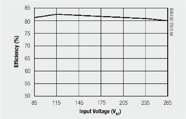
Fig. 3.273: Full load efficiency over input voltage
Key Design Points
T1 has a turns ratio (4.6) to ensure this circuit operates in discontinuous mode (DCM) at low line (85VAC) and D1 has a conduction time at least 4.5 µs.
Feedback resistors R1 and R2 have 1% tolerance values for tightly centering both the nominal output voltage and the CC regulation threshold.
RF1 acts as a fuse: Ensure it has a rating to withstand instantaneous dissipation when the supply is first connected to the AC. Use a wire wound or oversized metal-film resistor.
Preload resistor R4 maintains the output voltage under fault conditions such as a disconnected load.
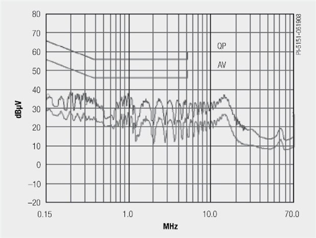
Fig. 3.274: Conducted EMI, 230 VAC input, EN 55015 B limits shown, output RTN floating
| Inductor parameters | |
| Core material | PC44, gapped for AL of 86,3 nH/t2 |
| Bobbin | Horizontal, 8 pins, EE10 |
| Winding details | Main Inductor: 97T x 34 AWG Tap Inductor: 27T, 27 AWG Feedback: 27T, 33 AWG |
| Winding order | Main Inductor (4-1), Tap Inductor (8-7) Feedback (6-5) |
| Total Inductance | 1.32mH, ± 10% |
| Primary resonant frequency | 1.1MHz (minimum) |
| Leakage inductance | - |
| Transformer parameters: (AWG = American Wire Gauge, TIW = Triple Insulated Wire) | |
Tab. 3.21: Inductor parameters
9.2.6 25 W quasi-resonant power supply
This section describes a solution for a 25 W power supply using the Green Mode FPSTM FSQ0365RL Fairchild Power Switch. The input voltage range is 160 VRMS – 265 VRMS and the is one DC output with 12 V/2.1 A. The power supply uses a quasi-resonant converter.