APPLICATION NOTE
ANP126 | Voltage specification for molded inductors
ANP126 by Annika Frankemölle, Alexander Lang
01. INTRODUCTION
1.1 Voltage and inductances
Inductors play a decisive role influencing the current rise in electrical circuits. In this process, the current resulting from the applied voltage induces a magnetic field, which opposes the current thus creating a controlled increase and can be limited as required. Therefore, when selecting the right inductor for an application, the inductance value and the maximum current rating needs to be considered, as they play a central role in the desired function of a switching regulator. Historically inductors in electrical circuits have used iron powder-based alloys or ferrite cores. For shaped cores, a coil former was used to secure the wire windings. The windings can be applied directly to toroids as the external epoxy coating serves as insulation in addition to protection against corrosion and moisture.. The selection of the insulation coating on enameled copper wire was primary based on temperature class rather than dielectric strength since the wire usually withstands several thousands of volts and had no direct contact with the core. This has changed in recent years with the increasing popularity of molded inductors based on fine iron powder with a distributed air gap where their design allows a wide range of sizes to be realized. The powder used for the core material consists of pure iron or iron powder-based alloys containing nickel, silicon or molybdenum, which are compressed under high pressure around the enameled copper winding using insulating synthetic resin as a binder. By constantly optimizing the production process and the material composition, it is possible to achieve the greatest possible permeability, in order to realize large inductance values in the smallest possible installation space. This must be combined with the maximum possible current carrying capacity. As a result, the power density per volume can be continuously increased. To constantly increase the power handling of the inductors in the smallest possible volume, the percentage of insulation binder in relation to the iron powder has been continuously reduced so that, consequently, the distance between the individual grain sizes has continuously decreased. This reduction has resulted in the fact that today, the applied voltages to an inductor within a DC-DC converter should be considered when selecting an inductor for an application, as the reduced insulating material content in the powder core limits the dielectric strength of the material and thus a high operating voltage can lead to failure of the entire application.
1.2 Trends and changes
As an example of the changing market conditions of electronics, the voltage drop across an inductor in a buck converter (Figure 1) will be considered below.
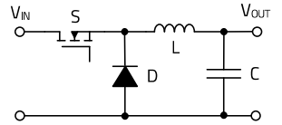
Figure 1: Reference schematic buck converter Vin = 24 V; Vout=5 V
At the moment of switching on, there is between 24 and 36 V at the input. The insulation of the powder particles must therefore be able to withstand 36 V permanently. With the continuous technological advancement in the semiconductor industry, MOSFETs today can achieve high power densities and fast switching speeds. As a result, it is now possible to reduce the output voltage in DC-DC converters in ever larger steps.
*An example: In the past, an input voltage of 48 V was gradually stepped down to 12 V, to 5 V and finally to 1.8 V. However, by using GaN MOSFETs in the application, it is possible to step down the voltage from 48 V directly to 1.8 V with enormously low switching losses (efficiency > 90%). With additional consideration of possible tolerances of the input voltage, up to 60 V can be applied to the inductor in the application at times. A value that high was rather usual in the past.
By using highly efficient MOSFETs, the designer thus has the advantage of being able to dispense with stage-by-stage regulation of the voltage, resulting in high-power density in a compact form. This allows the entire application to be further miniaturized and, as a result, costs can be saved. For this reason, the question of the dielectric strength of inductors has become very important in recent years when selecting the right inductor and will continue to be a requirement to be considered in the future. To ensure the necessary transparency, Würth Elektronik has decided to integrate the new operating voltage property for all powder-based storage inductors into the data sheets. For this purpose, a state-of-the-art testing concept was developed, which will be explained in more detail shortly.
02. DEFINITION OF THE OPERATING VOLTAGE
Würth Elektronik defines the maximum operating voltage Vop in their datasheets at which an inductor can be operated continuously during the application, without affecting the performance, risking damage, or overheating of the component. The operating voltage is therefore a limit value for the input voltage to which the inductor can be reliably used without irreversible damage in an application. The maximum operating voltage of a molded inductor can be influenced by various factors. For example, the inductance value of an inductor, ambient conditions, or the material composition. In addition, the design of the component can play a decisive role. For example, the arrangement of the winding layers of the coil and the insulation materials on the copper wire can have an impact on the maximum operating voltage.
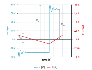
Figure 2: Inductor waveform – Delimitation Vp and Vop[1]
In contrast to the operating voltage Vop, the parameter of peak voltage Vp refers to the maximum voltage across the inductor without causing damage. The peak voltage can be applied across the inductor for a short period compared to the total “switch on-time”. During the switching operations in a buck converter for example, the voltage across the inductor exceeds the max operating voltage value for a short time (Figure 2). Parasitic effects of the MOSFETs and the inductor mainly cause this. An inductor used in this application needs to be able to withstand these short-term voltage peaks without taking damage or affecting the reliability of the circuit.
03. EFFECTS OF EXCEEDING THE OPERATING VOLTAGE
3.1 Influencing factors
As previously described, a steady optimization of the ratio between the powder and insulation binder led to a reduction of the dielectric strength. But what happens if the voltage is too high? To better understand this, the structure of a powder inductor is analyzed in more detail. Ferrite materials are ceramic compounds consisting of iron oxide (Fe2O3) in combination with other metal oxides such as manganese, nickel or zinc. After firing, these materials have a crystalline structure in which the iron and other metal ions are arranged in a specific lattice form. This crystalline structure inherently prevents the free movement of electrons, resulting in non-conductive behavior. Pressed powder or powder alloys consist for the most part of iron powder, which has very good electrical conductivity. Unlike traditional cores which have an external coating protecting them from the environment, the pressed core material is exposed (Figure 3).
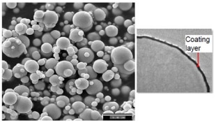
Figure 3: Microscopic analyze of a powder structure of a molded inductor [Zoom: 5µm] [2
Therefore, the particle coating needs to insulate electrically and protect against environmental influences because iron begins to rust as soon as it encounters atmospheric moisture and the electrical properties of the inductor would be lost. There are different types of coating for the desired area of application, such as resistance to chemical influences, temperature, or humidity. The thickness and the material of the coating resulting from the manufacturing process play an important role. However, this can lead to decreasing the power density per volume of an inductor at the same time. Reliability and electrical performance must be weighed to select the optimum ratio. Secondly, the binder that holds the individual particles together after the pressing process must also withstand the environmental influences. Particle coating and binder between the particles together form a barrier between the conductive parts of the component like the terminals. If this barrier is not sufficiently strong for the voltage used in the application, the consequence is that a conductive path is created through the core material by the individual metal particles. It can be seen in Figure 4 that the particles have been melted together after too high voltage was applied.
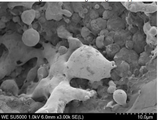
Figure 4: Microscopic analyze of a melted powder structure of a molded inductor [Zoom: 10µm]
3.2 Practical example
To illustrate the influence of not observing the maximum voltage on a real application a measurement setup was build up. What effect can an overvoltage have on the real application? For the experimental setup, two identical inductors were used. One of which had insulation damage provoked in advance with multiple voltage impulses over 200 V. The other inductor was taken directly from the reel. At first glance, no difference can be detected visually between the damaged and the intact part. Also, the error cannot be determined by measuring the electrical properties according to the data sheet (Figure 5).
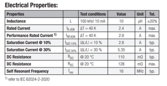
Figure 5: Current data sheet of the measured component
After measuring the inductance value and the RDC of both components, the electrical properties are still within the specification. It can be seen in Figure 6 that the voltage damage is not influencing the electrical parameter mentioned in the datasheet.
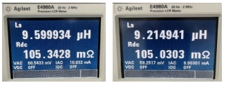
Figure 6: RDC and inductance measurement of component without voltage defect (left) and with voltage defect (right)
Both parts still work like normal according to the specification. Therefore, the existing specification of the data sheets is not enough. To show the influence of a damaged part, both were inserted into the circuit of a step-down converter, which converts an input voltage of 18 V to an output voltage of 5 V and an average output current of 1 A (Figure 7).
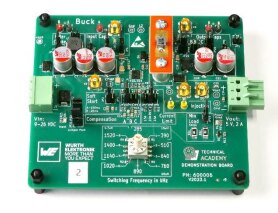
Figure 7: Picture of the test board (inductor mounted on the red PCB)
To evaluate the effect of insulation, damage the ripple current of the respective inductor is recorded (Figure 8). What can be seen is that the shape of the ripple current has changed compared to the good part. The reason for this is the conductive path in the core material caused by the overvoltage. There is now from a schematic point of few, a resistor in parallel to the inductor (Figure 9).
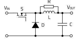
Figure 9: Illustration of the schematic resistor in parallel to the inductor
The new waveform is now the combination of these two components. The behavior of the inductor (green line) and the resistor (blue line) has been overlayed onto the diagram of the ripple current (Figure 10)
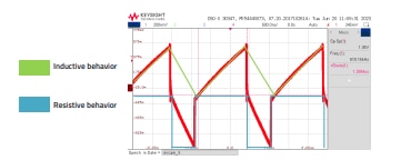
Figure 10: Behavior of the inductor (green line) and the resistor (blue line)
It can be shown that the application still works. The voltage is stepped down from 18 V to 5 V. But what is the influence of this resistor which has appeared in the schematic and in the ripple current diagram? The answer to this question can be found by checking the self-heating of the inductor. To compare the temperature rise of the inductor, a thermal camera was used to visualize the self-heating difference of both components (Figure 11). For the component without voltage damage the hotspot temperature is 42.9°C. This means during operation of the application the self-heating of the good inductor was about 20° K based on the ambient temperature, which is a reasonable value. In contrast the component with the voltage damage reached a hotspot temperature of 118.3°C. With the same test conditions, the damaged inductor had a self-heating of about 95°K. The losses of the inductor have risen more than 200%. The conductive path through the material causes several issues:
- DC losses: The current through the material, which is a resistor, causes pure losses. P = I² * R
- AC losses: The current through the material disturbs the magnetic field lines greatly increasing the eddy currents.
These additional losses reduce the efficiency of the inductor significantly. The advantage of a DC-DC converter to transfer voltage levels at high efficiency is lost.

Figure 8: Screen capture of the ripple current undamaged component (left) and damaged component (right)
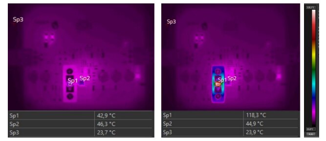
Figure 11: Self-heating recording of the undamaged component (left) and damaged component (right)
04. TEST METHOD
Determining the maximum operating voltage in an individual application is a challenge. A popular test method in production is pulse voltage tests to check the quality and reliability of components. However, this method cannot be used to determine the actual longevity of the components in an application. It is a snapshot, which may have already changed after the processing at the customer. Therefore, Würth Elektronik, in cooperation with a wellknown test house, has taken up the challenge of developing a concept that tests the behavior of the component at higher voltages close to the application and over a longer period. From this cooperation, a system was developed that uses the latest GaN switching technology to test an inductance within a full-bridge DC-DC converter (Figure 12). When the duty cycle is lower or higher than 50%, a DC bias voltage is built across the series capacitor.
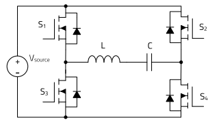
Figure 12: Schematic full-bridge buck converter [1]
The measuring device is thus able to feed the inductance with a square-wave voltage, which generates a triangular current and thus a magnetic flux. The function is identical compared to a regular DC-DC converter. The component can be tested under real life conditions. With the help of software, important parameters such as the inductance value, the total AC losses or the temperature rise, among others, can thus be determined during the measurement process. This allows the behavior of an inductance to be recorded over a long period of time, and any deviations that arise can be detected and analyzed. Thus, Würth Elektronik can make a statement whether the properties of the component change over time and to identify the maximum non-destructive operating voltage for an inductor. With the knowledge of the behavior of a DC-DC converter combined with the possibilities of the test application a procedure has been defined which stresses the DUT under real life condition.
4.1 Test description
To validate the operating voltage Würth Elektronik has performed tests for each individual series and size to be sure that all influential parameters such as material composition, dimensions, winding build up, production technology, etc. have been checked and taken into consideration. To stress the inductors up to their voltage limits, a very fast voltage transient up to 60 V/ns and with a switching frequency up to 2 MHz has been used to simulate the worstcase conditions [1]. To ensure a high load the testing device is always set up to use the highest switching frequency. After the setup of the specified input parameters such as the source voltage, duty cycle and frequency the test can be started. This has been done in a two-step procedure:
1. Check by a short-term test to evaluate the rough voltage resistivity of the molded inductor.
2. Define the operating voltage and prove it with a long-term test based out of the experience of the short-term test.
To ensure that all molded inductors not suffered any damage, pre- and post-measurements before and after every test run are carried out and compared. After the long-term test has been passed the molded inductor can be rated with its specific maximum operating voltage Vop in the datasheet. As an example, you can find the new datasheet specification of the electrical properties now for our series WE-MAPI (Figure 13)
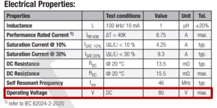
Figure 13: Example of a data sheet of the part number 74438356010HT
4.2 Analysis of the results
During the evaluation of the test procedure, it was discovered, that the voltage change on the inductor is more critical than a stable voltage for a short period of time. A differential high voltage over time causes a discharge because the dielectric permittivity (εr) of the material comes into play, i.e. the charge density becomes too high. The higher the switching frequency of a buck converter, for example, the higher the load on the pressed inductor caused by the partial discharge. When the voltage is high enough to cause such a partial discharge, it starts harming the insulation of the wire, the binder and the coating of the particles. In the test the peak voltage was also taken into consideration. During the switch-on phase , voltage peaks occur in the test setup, as the setup has the advantage of behaving electrically in the exactly same way as a real DC-DC converter By specifying an operating voltage this peak voltage has been checked and passed during the test. To establish a judgement criterion, the AC losses and the selfheating have been monitored continuously during the test. When both parameters stay within a defined tolerance band and both values are constant in this tolerance band, then by definition, that part is in a stable condition and there are no changes occurring which means there is not partial discharge to damage the insulation of the coating or the binder.
05. SUMMARY
As a result, with this innovative measurement technology Würth Elektronik is now able to provide the customer the maximum operating voltage for molded inductors as a guideline for their applications. The maximum operating voltage defined in the datasheets refers to the input voltage of a DC-DC converter. With this specification for operating voltage Würth Elektronik provides an additional service that applications can be designed according to the highest reliability standards. Therefore, aging effects are no longer a topic of concern. The peak voltage is not defined in the datasheets of the inductors. The reason being that this parameter can vary depending on the design. During the qualification procedure at Würth Elektronik a peak voltage of approximately 15% above the maximum operating voltage was found not cause any issue during the test. Higher peak voltages should be avoided in order not to damage the application. The user can use this value as a guide for selecting a suitable inductor.
A.1 References
[1] MindDCet NV: High Voltage Inductor Measurement System technical overview [internal] (2022).
[2] BASF Digital Solutions GmBH: Carbonyl Iron Powder [internal] (2022).
[3] Mike Wens and Jef Thoné: Characterizing High Voltage Inductors and Magnetic Material via Triangular Flux Excitation (2023).
IMPORTANT NOTICE
The Application Note is based on our knowledge and experience of typical requirements concerning these areas. It serves as general guidance and should not be construed as a commitment for the suitability for customer applications by Würth Elektronik eiSos GmbH & Co. KG. The information in the Application Note is subject to change without notice. This document and parts thereof must not be reproduced or copied without written permission, and contents thereof must not be imparted to a third party nor be used for any unauthorized purpose. Würth Elektronik eiSos GmbH & Co. KG and its subsidiaries and affiliates (WE) are not liable for application assistance of any kind. Customers may use WE’s assistance and product recommendations for their applications and design. The responsibility for the applicability and use of WE Products in a particular customer design is always solely within the authority of the customer. Due to this fact it is up to the customer to evaluate and investigate, where appropriate, and decide whether the device with the specific product characteristics described in the product specification is valid and suitable for the respective customer application or not. The technical specifications are stated in the current data sheet of the products. Therefore the customers shall use the data sheets and are cautioned to verify that data sheets are current. The current data sheets can be downloaded at www.we-online.com. Customers shall strictly observe any product-specific notes, cautions and warnings. WE reserves the right to make corrections, modifications, enhancements, improvements, and other changes to its products and services. WE DOES NOT WARRANT OR REPRESENT THAT ANY LICENSE, EITHER EXPRESS OR IMPLIED, IS GRANTED UNDER ANY PATENT RIGHT, COPYRIGHT, MASK WORK RIGHT, OR OTHER INTELLECTUAL PROPERTY RIGHT RELATING TO ANY COMBINATION, MACHINE, OR PROCESS IN WHICH WE PRODUCTS OR SERVICES ARE USED. INFORMATION PUBLISHED BY WE REGARDING THIRD-PARTY PRODUCTS OR SERVICES DOES NOT CONSTITUTE A LICENSE FROM WE TO USE SUCH PRODUCTS OR SERVICES OR A WARRANTY OR ENDORSEMENT THEREOF. WE products are not authorized for use in safety-critical applications, or where a failure of the product is reasonably expected to cause severe personal injury or death. Moreover, WE products are neither designed nor intended for use in areas such as military, aerospace, aviation, nuclear control, submarine, transportation (automotive control, train control, ship control), transportation signal, disaster prevention, medical, public information network etc. Customers shall inform WE about the intent of such usage before design-in stage. In certain customer applications requiring a very high level of safety and in which the malfunction or failure of an electronic component could endanger human life or health, customers must ensure that they have all necessary expertise in the safety and regulatory ramifications of their applications. Customers acknowledge and agree that they are solely responsible for all legal, regulatory and safety-related requirements concerning their products and any use of WE products in such safety-critical applications, notwithstanding any applications-related information or support that may be provided by WE. CUSTOMERS SHALL INDEMNIFY WE AGAINST ANY DAMAGES ARISING OUT OF THE USE OF WE PRODUCTS IN SUCH SAFETYCRITICAL APPLICATIONS.
DIRECT LINK
ANP126 | Voltage specification for molded inductors
USEFUL LINKS:
Application Notes : https://we-online.com/en/support/knowledge/application-notes
Services: https://we-online.com/en/products/components/service
Contact : https://we-online.com/en/support/contact
CONTACT INFORMATION
Würth Elektronik eiSos GmbH & Co. KG
Max-Eyth-Str. 1, 74638 Waldenburg, Germany
Tel.: +49 (0) 7942 / 945 – 0
Email: appnotes@we-online.de

