


APPLICATION NOTE
Filter and surge protection for I2C Bus
ANP121 by Andreas Nadler
01. INTRODUCTION
The I²C (Inter-Integrated Circuit) bus is a popular serial communication interface on many circuit boards. It is mainly used to connect microcontrollers with peripheral ICs (e.g. sensors or memory). The bus uses a bidirectional data line (SCL) and clock line (SDA) respectively. However, the I²C bus is not only used on circuit boards. In many applications, the I²C bus is extended into other areas using various connectors and cables. This makes the I²C bus potentially more susceptible to external interference such as ESD, burst and radiated RF. The goal of this application note is to show the reader a suitable filter and protection circuit that increases the noise immunity of the I²C bus without sacrificing the signal quality of the data and clock lines. For this purpose, simulation models were created in LTspice and a real application was measured to verify the simulation results.
02. OVERVIEW I2C BUS

Figure 1: Simplified block diagram I2C bus
The I²C operates according to the "master-slave" principle, whereby the master always initiates the data transfer. Due to its low complexity, the bus has achieved a wide distribution. However, the protocol is very simple, and the physical topology is only single-ended. In practice, both of these factors mean that the bus can be very susceptible to external interference (e.g. during EMC tests).
03. OVERVIEW I²C SPECIFICATIONS
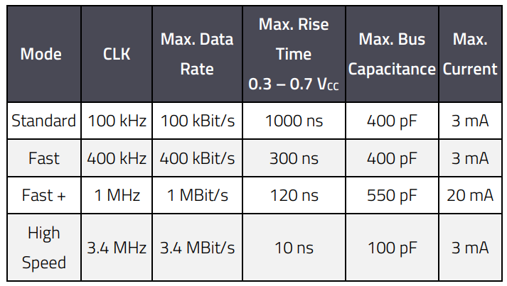
Table 1: Overview I2 C bus specifications
04. PULL-UP RESISTORS, BUS CAPACITANCE AND RISE TIME
All ICs that participate in the I²C bus have open collector outputs. These switch the pull-up resistors alternately to reference ground and thus generate the logical states "1"(VCC) and "0"(GND). As can be seen in Table 1, the maximum permissible edge rise times decrease as the data rate increases. The mathematical relationship of the min./max. values for the pull-up resistors is as follows:
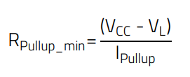 (1)
(1)
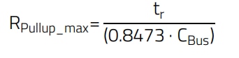 (2)
(2)
| VCC = | Reference voltage level of the I²C-Bus (Volt) |
| VL = | Maximum logic „0“ threshold level (e.g. 0.4 V at VCC > 2 V) (Volt) |
| CBus = | Maximum logic „0“ threshold level (e.g. 0.4 V at VCC > 2 V) (Volt) |
| tr = | Maximum allowed rise time (depending on data rate) (seconds) |
| IPullup = | Maximum allowed rise time (depending on data rate) (seconds) |
The pull-up resistors in combination with the parasitic bus capacitance form an RC element. This leads to a delay of the edge rise time of the square signal. In many applications, this RC element is often the limiting factor regarding the maximum possible data rate and cable length. As shown in Table 1, the I²C specification therefore results in a maximum bus capacitance of 400 pF at 3 mA current for the most commonly used data rates (100 kBit/s & 400 kBit/s). The smaller the pull-up values are selected, the shorter the edge rise time can become. As can be seen in equation (1), the lower limit determines the maximum logic low threshold, the voltage reference level and the maximum possible current.
The parasitic bus capacitance depends on, among other things:
- Component capacitance
- Length and width of traces (approx. 0.5 pF/cm)
- Length, type of cable and connectors
- Layer structure and dielectric constant of the PCBs
05. SELECTION OF THE FILTER AND OVER VOLTAGE PROTECTION COMPONENTS

Figure 2: I²C bus including interface protection for improved noise immunity and reduced interference emission
To increase immunity to ESD, burst and radiated RF, a combination of SMT ferrites plus TVS diodes can be used. Wideband SMT ferrites (e.g. 742792693) continuously build up impedance above 10 MHz and are therefore able to protect the bus against high-frequency interference. Overvoltages can also be effectively diverted to reference ground by the TVS diodes. Since the values of the pull-up resistors are often in the kΩ range, the RDC as well as the impedance of SMT ferrites below 10 MHz only play a minor role here. Thus, in a first consideration, it can be assumed that the edge rise time of the useful signal is hardly influenced in practice. If suitable TVS diodes with low capacitance (e.g. 824012823 - 0.18 pF) are selected, their component capacitance also has no relevant influence on the signal quality.
During an ESD test, for example, a current of more than 10 A can flow briefly, which then leaves a voltage of about 10 V at this diode. All other ICs on the I²C bus must then withstand this voltage. This only works if a low-impedance ground (e.g. large copper area in an inner layer) is provided to avoid a further voltage drop.
06. LTSPICE SIMULATION WITH 400 KHZ CLOCK RATE
With the help of the free simulation program LTspice it is relatively easy to investigate the influence of the parasitic bus capacitance in combination with the selected pull-up resistors. In order to generate the desired useful signals, it is advisable to use a voltage-controlled switch. With the help of the voltage source practically any periodic signal can be generated. For this purpose, the "Pulse" function is selected and the desired bandwidth is determined on the basis of the desired I²C specification. For the widely used 400 kBit/s variant, a period duration of 2.5 µs is selected. For a 50% duty cycle, the "high" time is set to 1.25 µs. In order to determine the edge steepness of the signal, one needs to get the rise times from the datasheets of the ICs being used on the bus. To be able to use the maximum allowed 400 pF parasitic bus capacitance, the pull-ups were set to 1 kΩ. Three channels (may represent SCL or SDA in practice) are simulated:
- Without parasitic bus capacitance
- 400 pF parasitic bus capacitance
- 400 pF + wideband multilayer SMT ferrite (742792693)
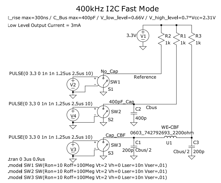
Figure 3: Schematic LTspice simulation with 3 channels --> 0 pF, 400 pF & 400 pF + Multilayer SMT Ferrite
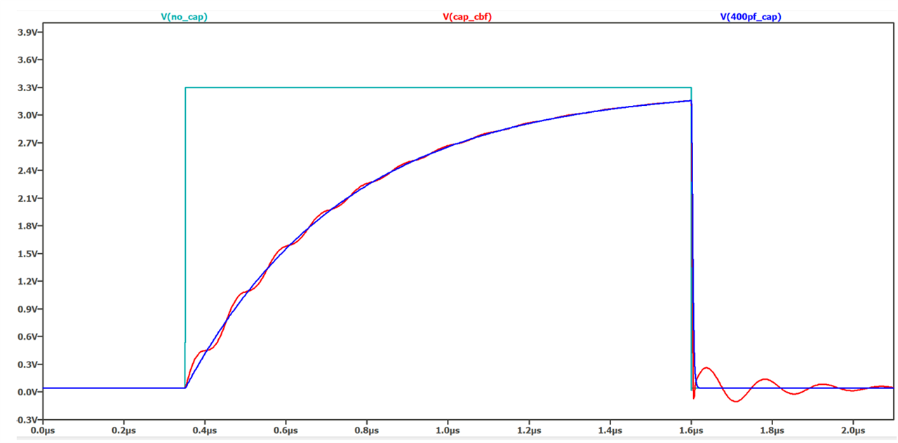
Figure 4: LTspice simulation result time domain 0 pF (Turquoise), 400 pF (Blue) & 400 pF+ Multilayer SMT Ferrite (Red)
The simulation result shows that practically no influence on the rise time of the signal can be expected from the multilayer SMT ferrite. Because each multilayer SMT ferrite also has an inductance component, minor oscillations are visible in combination with the bus capacitance. However, these are not critical because their amplitudes are less than 10% of the actual useful signal. In the real measurements, these oscillations are significantly lower.
07. MEASUREMENT OF A REAL APPLICATION WITH 400 KHZ CLOCK RATE
To verify the relatively simple LTspice simulation, additional measurements were performed on a Würth Elektronik SensorBLE FeatherWing Kit. (Figure 5)
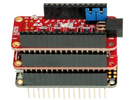
Figure 5: : Würth Elektronik SensorBLE FeatherWing Kit
This kit consists of a master board, which contains the microcontroller. The other two contain a WE Bluetooth module and various WE sensors (3-axis acceleration, temperature, humidity, pressure). The master board communicates with the other two via I²C bus at a maximum data rate of 400 kBit/s. The sensor data can then be visualized with a suitable smartphone app (WE-SensorBLE). A parasitic capacitance of 400 pF with respect to GND was simulated using MLCCs. The same multilayer SMT ferrite (742792693) was used as in the simulation, plus a TVS diode array (824012823). In addition, 20 cm of cable was used to connect the sensor board to the rest of the I²C. Such an arrangement can be observed in many applications in practice.
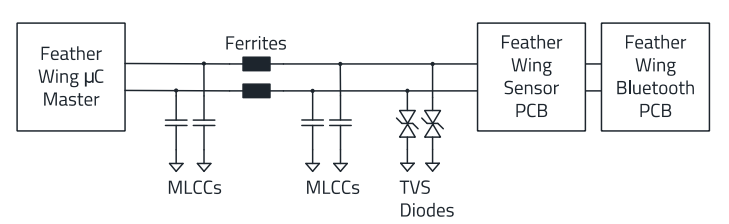
Figure 6: Block diagram test setup with Würth Elektronik SensorBLE FeatherWing Kit
The voltage curve on the SCL line was always measured.
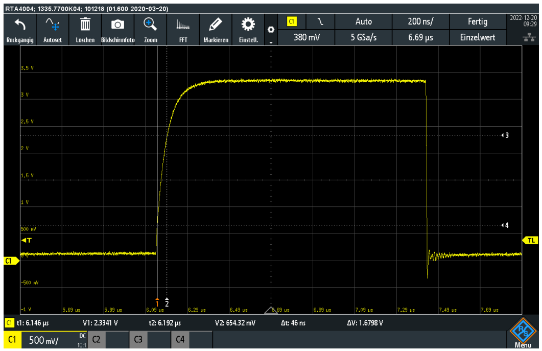
Figure 7: Reference measurement with 1 kΩ pull-ups without further changes of the used FeatherWing hardware (= 46 ns rise time)
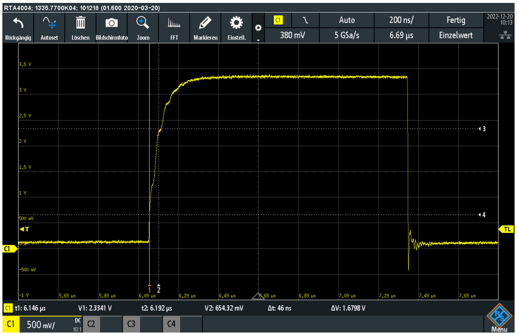
Figure 8: : Reference measurement with 1 kΩ pull-ups + multilayer SMT ferrite + TVS diode array + 20 cm cable (= 46 ns rise time)
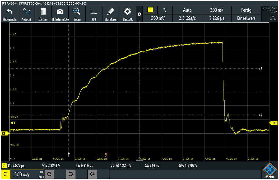
Figure 9: Reference measurement with 1 kΩ pull-ups + multilayer SMT ferrite + TVS diode array + 20 cm cable + 400 pF MLCCs (= 344 ns rise time)
The measurements show practically identical results to the simulation. The rise time and signal quality are not negatively affected by the multilayer SMT ferrite in combination with the TVS diode. The rise time of the high signal, which is critical for the timing, depends only on the bus capacitance in combination with the selected pull-up resistors. Using the smartphone app (WE-SensorBLE), errorfree operation could be verified in all three tested scenarios.
08.SUMMARY
In this application note it was shown by simulation and measurement that SMT multilayer ferrites in combination with ESD protection diodes practically do not influence the data signal (SDA) and clock signal (SCL) of the I²C bus. The edge steepness of the signals is mostly influenced by the pull-up resistors in combination with the parasitic bus capacitance. In return, this component combination of ESD protection diode and broadband SMT ferrite increases the noise immunity of the I²C bus. In practice, this means a higher immunity to ESD, burst and radiated RF.
A Appendix
A.1 Bill of material (BOM)

A.2 Relevant standards
ESD Test: DIN EN 61000-4-2 / IEC 61000-4-2
Burst Test: DIN EN 61000-4-4 / IEC 61000-4-4
Eingestrahlte HF: DIN EN 61000-4-3 / IEC 61000-4-3
A.3 References
SLVA689 – I 2C Bus Pull-up Resistor Calculation
IMPORTANT NOTICE
The Application Note is based on our knowledge and experience of typical requirements concerning these areas. It serves as general guidance and should not be construed as a commitment for the suitability for customer applications by Würth Elektronik eiSos GmbH & Co. KG. The information in the Application Note is subject to change without notice. This document and parts thereof must not be reproduced or copied without written permission, and contents thereof must not be imparted to a third party nor be used for any unauthorized purpose. Würth Elektronik eiSos GmbH & Co. KG and its subsidiaries and affiliates (WE) are not liable for application assistance of any kind. Customers may use WE’s assistance and product recommendations for their applications and design. The responsibility for the applicability and use of WE Products in a particular customer design is always solely within the authority of the customer. Due to this fact it is up to the customer to evaluate and investigate, where appropriate, and decide whether the device with the specific product characteristics described in the product specification is valid and suitable for the respective customer application or not. The technical specifications are stated in the current data sheet of the products. Therefore the customers shall use the data sheets and are cautioned to verify that data sheets are current. The current data sheets can be downloaded at www.we-online.com. Customers shall strictly observe any product-specific notes, cautions and warnings. WE reserves the right to make corrections, modifications, enhancements, improvements, and other changes to its products and services. WE DOES NOT WARRANT OR REPRESENT THAT ANY LICENSE, EITHER EXPRESS OR IMPLIED, IS GRANTED UNDER ANY PATENT RIGHT, COPYRIGHT, MASK WORK RIGHT, OR OTHER INTELLECTUAL PROPERTY RIGHT RELATING TO ANY COMBINATION, MACHINE, OR PROCESS IN WHICH WE PRODUCTS OR SERVICES ARE USED. INFORMATION PUBLISHED BY WE REGARDING THIRD-PARTY PRODUCTS OR SERVICES DOES NOT CONSTITUTE A LICENSE FROM WE TO USE SUCH PRODUCTS OR SERVICES OR A WARRANTY OR ENDORSEMENT THEREOF. WE products are not authorized for use in safety-critical applications, or where a failure of the product is reasonably expected to cause severe personal injury or death. Moreover, WE products are neither designed nor intended for use in areas such as military, aerospace, aviation, nuclear control, submarine, transportation (automotive control, train control, ship control), transportation signal, disaster prevention, medical, public information network etc. Customers shall inform WE about the intent of such usage before design-in stage. In certain customer applications requiring a very high level of safety and in which the malfunction or failure of an electronic component could endanger human life or health, customers must ensure that they have all necessary expertise in the safety and regulatory ramifications of their applications. Customers acknowledge and agree that they are solely responsible for all legal, regulatory and safety-related requirements concerning their products and any use of WE products in such safety-critical applications, notwithstanding any applications-related information or support that may be provided by WE. CUSTOMERS SHALL INDEMNIFY WE AGAINST ANY DAMAGES ARISING OUT OF THE USE OF WE PRODUCTS IN SUCH SAFETYCRITICAL APPLICATIONS
DIRECT LINK
ANP121 | Filter and surge protection for I²C Bus
USEFUL LINKS:
Application Notes : https://we-online.com/en/support/knowledge/application-notes
Services: https://we-online.com/en/products/components/service
Contact : https://we-online.com/en/support/contact
CONTACT INFORMATION
Würth Elektronik eiSos GmbH & Co. KG
Max-Eyth-Str. 1, 74638 Waldenburg, Germany
Tel.: +49 (0) 7942 / 945 – 0
Email: appnotes@we-online.de