


It´s a match - The difference of a matched vs. unmatched antenna
By Sofie-Marie Wacker
As a manufacturer of chip antennas, we as Würth Elektronik eiSos want to show our customers, how their antennas work. So we asked ourselves the question: how can we visualize antenna performance? Like many electrical parameters, electromagnetic waves are invisible to the human eye. The goal of this project was to create an application, that we could bring to customer seminars to show antenna performance in an easy way without external measurement equipment. Here, we want to show also how the range and signal intensity changes with a change of the size of the chip antenna and the influence of antenna matching.
Würth Elektronik already offers a broad range of FeatherWing modules, including the Thyone-I Wireless FeatherWing Module. It offers a secure 2,4 GHz proprietary wireless connectivity solution. The demoboard for antenna visualization should use Bluetooth technology. But the foundation is fixed: Use the existing Thyone wireless FeatherWing, change it according to our requirements and add a Chip Antenna. From our portfolio, I chose four electric antennas in the 2,4 GHz frequency band with different dimensions. In table 1 you can see, the peak gain is correlated with the dimensions of the chip antenna. Here, customers have to choose between performance, size and price. In general, chip antennas have a very good size to performance ratio and should definitely be considered if the space of the application is limited.
|
Article Number |
Farnell Ordercode |
Size [mm] |
Impedance [Ω] |
Gpeak [dBi] |
VSWR [%] |
|
3,2 x 1,6 |
50 |
0,5 |
2,00 |
||
|
5,2 x 2,1 |
50 |
2,5 |
2,00 |
||
|
7,0 x 2,0 |
50 |
2,7 |
2,00 |
||
|
9,0 x 2,0 |
50 |
3,0 |
2,00 |
Table 1: Electrical parameter of the four chosen Antennas
Now we come to the part of designing the antenna on the existing FeatherWing module. The space is too tightly packed to place the antenna according to our design rules. There, we have a simple workaround: make the PCB bigger. The PCB becomes longer as the outer dimensions on the longer side are limited by pin headers.
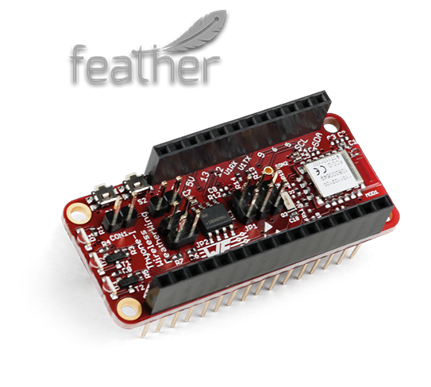
Figure 1: WE-Thyone-I Wireless FeatherWing Module
The gained space is needed to not only place the antenna, but also the matching circuit and an UMRF connector. The UMRF connector is only needed for the matching phase and can be left off a matched FeatherWing. With this, we can ensure a decoupled connection to the measurement device. The proposed matching network is a combination of a Pi and T-network to ensure maximum flexibility in the matching process.
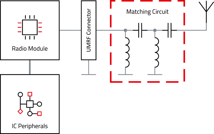
Figure 2: Typical antenna feeding network
The antenna should be placed as close as possible to the radio module to keep the feeding line as short as possible. The layout in Figure 3 it is not ideal because the outport for external antennas is located to the upper side. Other design rules are:
- Cut out copper in all PCB layers under the antenna
- Design the matching circuit for component size 0402
- Design the feed line if the antenna to the impedance of 50 Ohm
To shield the antenna from influences, a via fence around the transmission line and on the edge of the HF part of the PCB is placed. Figure 3 shows the result of the implemented changes. The area around the chip antenna is free from the copper plane. The UMRF connector is marked in turquoise. It is placed between the radio module and the matching network. The HF pin is placed directly on the feeding line to ensure signal integrity.
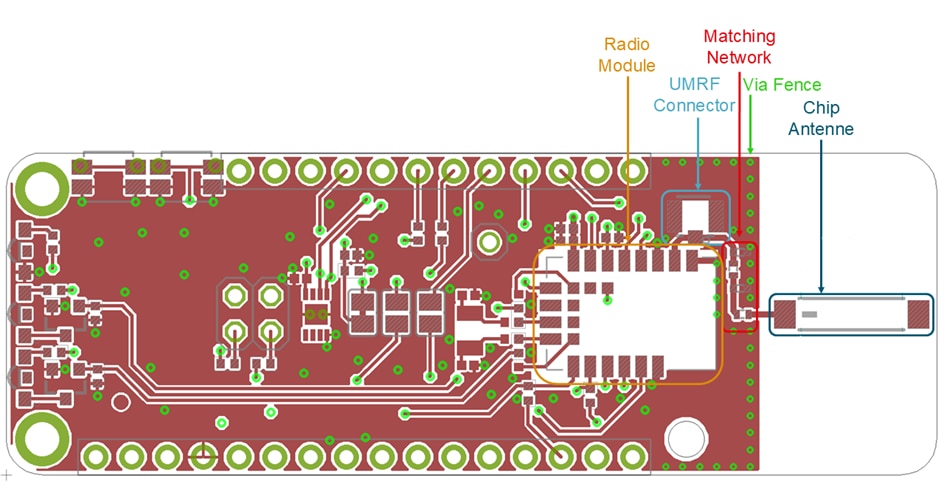
Figure 3: PCB Layout of FeatherWing with Chip Antenna
The next step is to match the antenna impedance to the feeding line impedance. Ideally both should be 50 Ohm. If the impedance does not match, the signal will be reflected and will not get transmitted by the antenna. This affects the performance.
The matching is done with passive components: inductors and capacitors in 0402 size. This size still allows comfortable soldering and desoldering of the components. For the matching, the Capacitor Kit and Inductor Kit from Würth Elektronik are used. These design kits contain all the essential values required for matching a chip antenna. An important accessory for matching is the smith chart. Every impedance value of any measured frequency can be shown on the chart. The smith chart acts like a coordinate system for real and imaginary parts of the impedance.
The goal is to get as close as possible to the middle of the smith chart for the frequency 2,45 GHz. The passive components have following influence on the impedance:
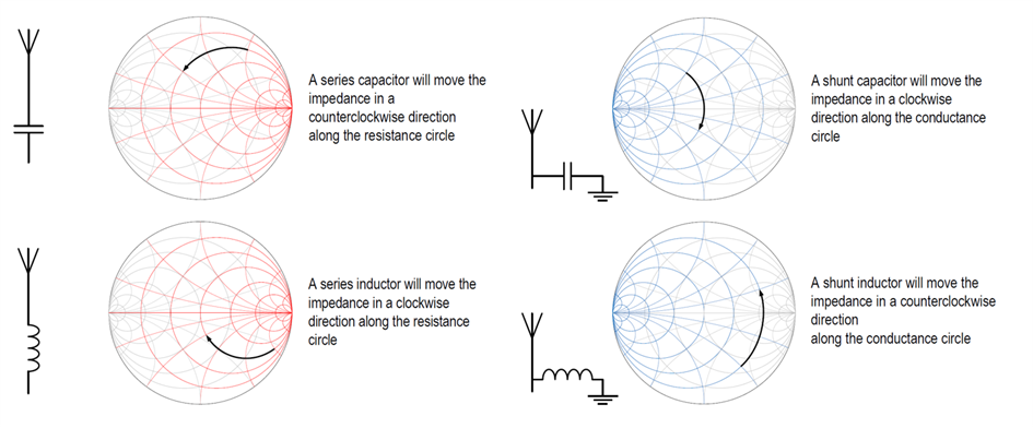
Figure 4: Influence of capacitors and inductors on impedance on the smith chart
The first step in a matching is analyzing the impedance without matching. The matching footprints serial in the feed line are shorted. As an example, we are taking a closer look at 74889502450. This is a relatively small antenna that has a good performance nonetheless. For the measurement we need a 1 port network analyzer. The network analyzer measures s-parameters and displays it in different views. In yellow we have reflection coefficient S11, voltage standing wave ratio (VSWR) in turquoise, efficiency in purple and the impedance in the smith chart.
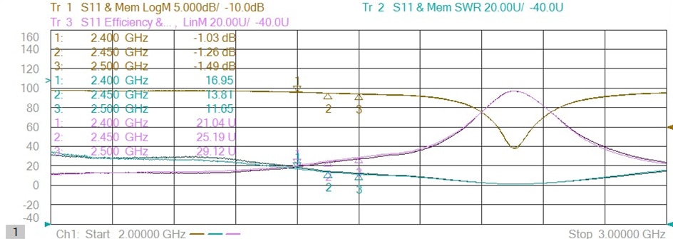
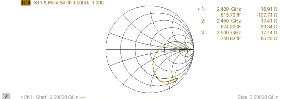
Figure 5: MCA 74889502450 on PCB without matching
Reminder: the goal is to move the impedance of 2,45 GHz (Marker 2) to the middle of the smith chart. The ideal impedance is 50 Ω + j0 Ω. As you can see in Figure 5, the impedance is far from perfect. It is near the bottom right border of the circle. The impedance value is 17.41 Ω - j96.34 Ω. To decide on the components to get to the middle, we use a tool which calculates the inductance or capacitance value. The user only has to decide which path to use. In theory there are infinite ways to reach the middle. But to get to the exact middle point is impossible. Due to tolerances and measurement inaccuracies, the parts will not follow the calculation exactly. Sometimes not even remotely.
A possible way to reach 50 Ω is shown in Figure 6. A series inductor of 4.7 nH shifts the impedance to 17,41 Ω - j24,035 Ω. A parallel inductor of 2.4 nH shifts the impedance to the desired value of 50 Ω.
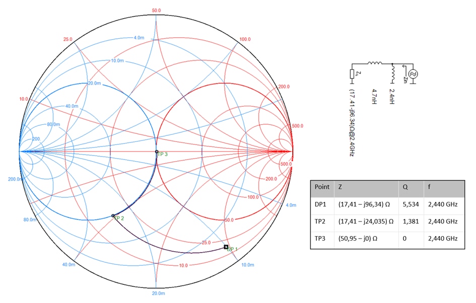
Figure 6: Proposed matching circuit
After theory comes practice which is often different in high frequency. The soldering of a series inductor of 4.7 nH causes a shift in the desired direction. A measurement with the network analyzer shows that the change is too much. With this knowledge, the inductance is changed to 3 nH. With this serial inductance, the impedance is 22.05 Ω - j37,12 Ω. Now, the goal is to reach 50 Ω with the parallel inductor. The initial calculation predicts a 2,4 nH parallel inductor. With the newly reached impedance, a new calculation has to be done. The new calculation proposes a 3.3 nH parallel inductor. The measurement shows, that the change with this value is too low. In a parallel inductor, the higher the inductance value, the smaller the change in impedance. The inductance value is changed in small steps until we reach the desired value. The smallest value of 1 nH finally results in a good matching. Figure 7 shows the final matching network with the inductance values that were used.
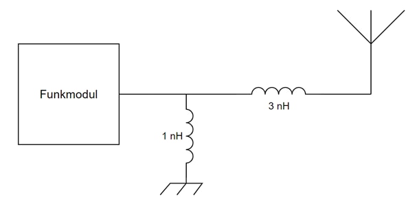
Figure 7: Matching network for the PCB
In general, the goal is to achieve a minimum reflection coefficient of -10 dB to call it a good matching. This should be achieved across the entire required frequency band that is used. In Figure 8 you can see the measurement with the matched antenna.
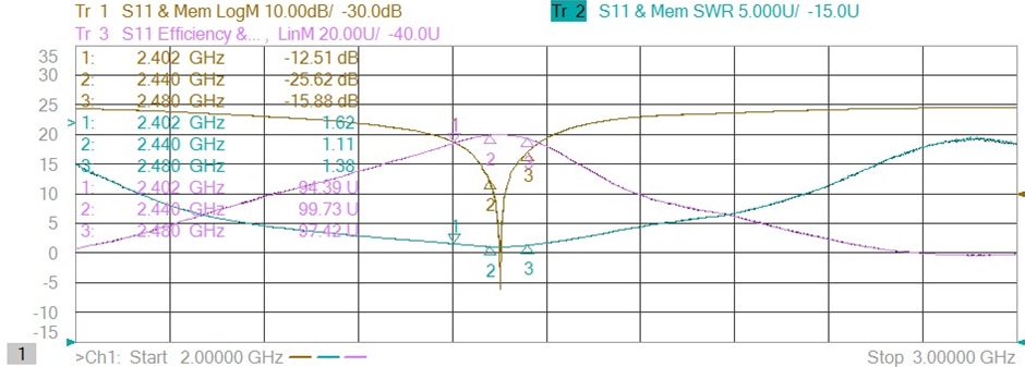
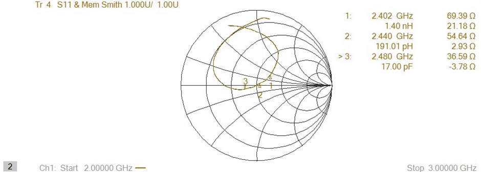
Figure 8: MCA 74889502450 on PCB with matching
The marker at 2,44 GHz is close to the middle. The impedance is 54.64 Ω + j2.93 Ω. The influence of the matching can also be seen in the top half of the picture. The bandwidth is bigger than before the matching. At 2,44 GHz the reflection coefficient is -25.62 dB. In the frequency range of Bluetooth, the minimum reflection coefficient is -12.51 dB. The marker catches a minimum VSWR of 1.11. But the graphs in the upper half of Figure 8 show that the resonance frequency is shifted upwards. If it would be closer in the middle, the performance could be even better. But the bandwidth is wide enough to have a good reflection coefficient across the whole required frequency band.
Each application and each antenna, requires a new matching. The impedance of the feed line can differ and of course environmental factors like the housing influence the antenna performance. Like explained, a matching can be time consuming and a developer needs equipment like a network analyzer. For our customers that use our antennas or radio modules, Würth Elektronik offers a free antenna matching service. All information regarding this service can be found on the website.
In this case, the performance is measured in distance and RSSI value. The RSSI value as a measure of the signal strength of a wireless transmission. There is no general definition. WE uses the absolute definition in dBm. The IEEE 802.15.4 standard requires ‑85 dBm sensitivity for a working data transmission. In this test setup we measure the distance until the connection is lost, which is often more than -85 dBm. The signal strength is tracked with the WE Bluetooth LE Connect App.
The measurement takes place in free field where no influences interfere with the signal. To minimize the influence of the ground the FeatherWing is placed in 125 cm height on a wooden stative. Figure 9 shows the test setup.
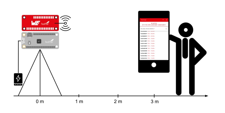
Figure 9: Test setup of RSSI value over distance
Based on an example, the performance is evaluated. Goal is to show, if the range improves with matching. Every two meters, a new RSSI value is tracked. With these values, we can create a graph of RSSI over distance. To compare antenna matching, we do this measurement twice: with and without matching. For this test, the biggest antenna of the four 74889102450 is used.
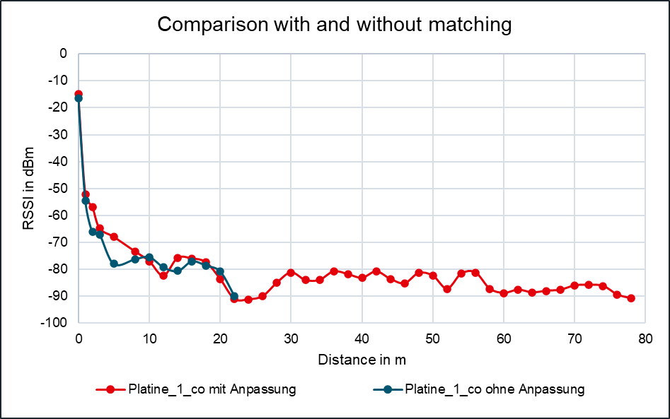
Figure 10: Comparison of 74889102450 with and without matching.
Both values start at the same level. The RSSI value drops for both PCBs in an exponential curve. The values stay the same until 22 m. Here, the expectation was a lower RSSI value from the non-matched antenna. Receiving signals from the FeatherWing without matching stops after 22 m. With the matched antenna on a PCB, this range goes up to 78 m. To summarize we can say: In this test we showed that matching improves the range by a factor of 3.5. This is of course only valid for this application but it gives us a feeling which parameters are influenced.
For another example we have the antenna 74889302450 on the corresponding board. Here, we want to test the difference between matchings. The result can be seen in Figure 11.
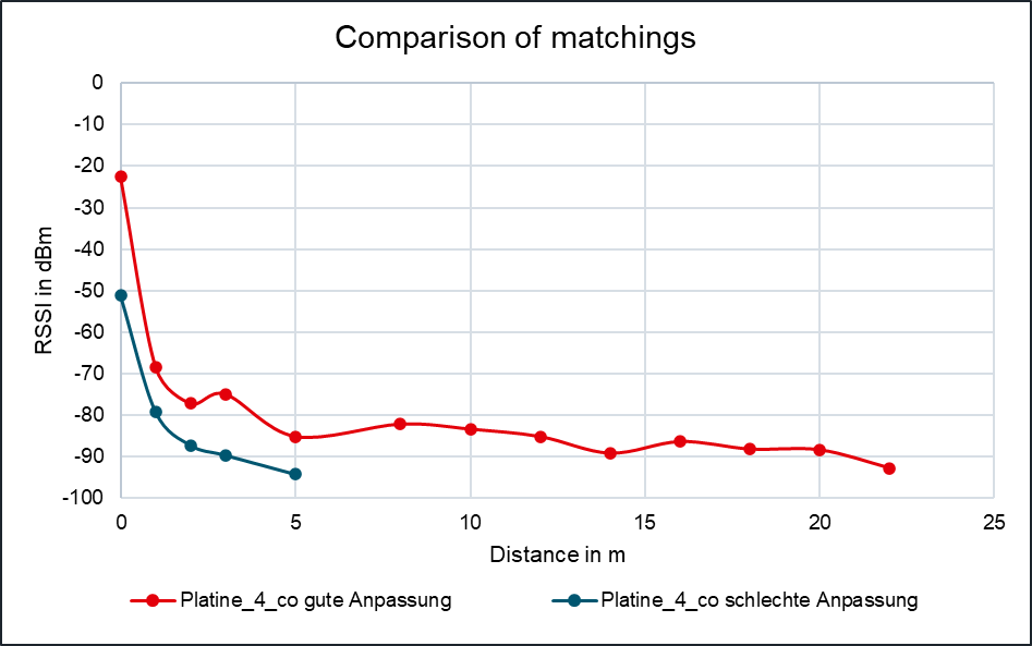
Figure 11: Comparison between matchings for 74889302450
The red line indicates a better matching, while the dark blue line indicates a worse matching. If we take a look at the S11 Parameter measurement we can analyze the background of these results. In Figure 12 we see the measurement results of these PCBs. On the left side is the result of the blue line. On the right side we can see the measurement of the red line.
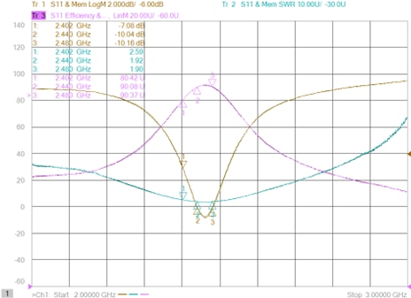
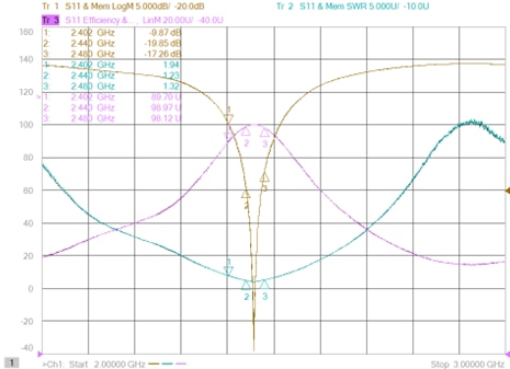
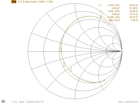
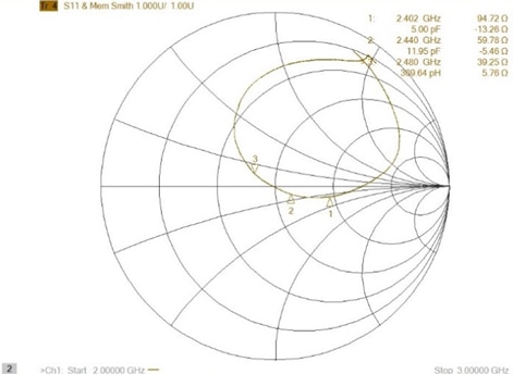
Figure 12: Comparison of the VNA measurements
In the left Smith Chart, the Impedance for 2,44 GHz is 38,68 Ω - j13,41 Ω. This is not very close to our goal of 50 Ω. Nonetheless, the reflection coefficient peak has the desired frequency. The maximum S11 value is around -11 dB. The frequency band is much broader than needed, indicating high losses. On the other hand, the high value frequency band of the S11 value is much narrower. The peak value of the reflection factor is -20 dB for marker 2 but much higher at a slightly higher frequency. We can also analyze the efficiency with the purple curve. On the left, the curve is not that sharp but generally on a higher level. On the right, the curve is more pointed towards the desired frequency. The other frequencies have a lower efficiency. This means unwanted frequencies are damped and the main frequency is radiated.
To summarize, the project showed that matching improves especially the range. Without matching, the range in free field is limited, whereas a simple matching with e.g. two parts can increase range considerably. Matching should be done in an exact way as Figure 11 shows a drop in antenna performance for “bad” matchings. The outer dimensions of a chip antenna also have influence on performance. The bigger the part the better the performance usually.

