onsemi and Würth Elektronik: 25kW DC Fast Charger Technology
Author: Octavian Stroe – Product Definition Engineer, Würth Elektronik
EV Charging Growth
The market for electric vehicles is booming: more and more electric vehicles on the road means that a comprehensive and demand-oriented charging infrastructure for electric vehicles is becoming increasingly important. Whether at home, at work, or on the road, an optimal and attractive range of charging options is indispensable. The long-term goal is to successfully integrate and establish electric mobility in our everyday lives.
The global EV charger market is expected to witness a burgeoning growth in the forthcoming years owing to the various factors such as surging sales of electric vehicles across the globe, rising demand for zero emission vehicles, and growing government initiatives to foster the adoption of electric vehicles. The governments in various developed and developing nations, such as China, Canada, Japan, and India, are offering subsidies to consumers to boost the adoption of electric vehicles.
The higher dependence on biofuels has resulted in increased levels of air pollution and, consequently, the prevalence of various respiratory and other diseases is surging among the global population. Curbing the carbon footprint and shifting towards clean and green energy are the major factors that are expected to drive the growth of the global EV charger market. The increasing consumer awareness regarding carbon emission from vehicles, increased environmental consciousness, improvements in the standard of living, and growing adoption of advanced technologies are altogether propelling the growth of the global EV charger market.
The technological developments in the electric vehicle and charging infrastructure such as ultra-fast chargers, portable charging stations, load management with smart charging, automated payment systems for charging, and bi-directional charging are expected to foster the growth of the EV charger market across the globe. onsemi and Würth Elektronik have partnered together to create a design for a 25kW bi-directional fast charger that can help meet this growing demand.

Figure 1. Projected Growth of EV Charger Market from 2022-2032
25kW Fast Charging Design

Figure 2. onsemi and Würth Elektronik‘s 25kW Fast Charger Design
The work for this design started with the definition of the actual DC charger power stage based on the requirements for the application. These are per the market’s needs and follow the guidelines of IE-68515.
The architecture of such power blocks is as follows: an AC-DC Power Factor Correction (PFC) stage at the front end, followed by a bi-directional DC-DC stage that provides isolation between the grid and the load (battery of the EV) and regulates the voltage and current at the output.

Figure 3. 25kW Charger Block Diagram
The three−phase six−switch active rectification stage helps achieve the 0.99 power factor correction (PFC) requirement with a total harmonic distortion below 7%, which are standard requirements in commercial DC charger systems. This delivers a highly efficient bidirectional solution with a low component count. Overall, this two−level architecture brings a superior cost−performance ratio while achieving the system requirements. The DC link will operate at a high−voltage 800 V to reduce peak currents, maximizing efficiency and power density. This requires 1200−volt VBD (Voltage Breakdown) power switches with two−level architecture. The switching frequency of the system is set at 70 kHz to keep the second harmonic below 150 kHz, keeping conducted emissions at bay and facilitating compliance with the EN 55011 Class A (EU) and FCC Part 15 Class A (US) norms (applicable to systems connected to the AC grid). These norms limit the degree of conducted emissions injected into the grid. Such an approach simplifies the complexity of the EMI filter and renders off−the−shelf solutions a good fit, which fulfills the purpose of the project.
The converter operates at 100 kHz, a compromise to keep the switching losses at a reasonable level as well as the core and AC losses of the magnetic components. Furthermore, the system will run flux−balancing control on the transformer. This technique removes the requirement for a bulky series capacitor to work with the transformer in Dual Active Bridge phase−shifted architectures. The flux−balancing control strategy helps reduce the system’s size, weight, and cost.

Figure 4. Power derating in alignment with DC charging profiles
In the e-mobility ecosystem, direct-current (DC) chargers provide “fast” and “ultrafast” charging capabilities, in contrast with slower alternating current (AC) chargers. In essence, EV chargers convert the AC power from the grid into DC power suitable for delivery into the batteries of the EVs. The power conversion in DC charging is handled outside the EV (“off−board”) and then delivered to the vehicle with power levels ranging from a few kW to more than 350 kW (with even higher levels in development). Higher-power DC chargers are built modularly, stacking power blocks of 15 to 75 kW (and above) in a single cabinet. In general, output voltages of DC chargers range from 150 V to above 1000 V, covering both the 400 V and 800 V standard EV battery levels and may be optimized for the higher or lower voltage end.
What goes into the design?
The onsemi’s 25kW charger benefits from new products designed specifically with the advance in SiC usage and stringent requirements in mind. With support from the onsemi design team, our new parts are tailored to the market requirements of such designs. Best-in-class performance versus cost is achieved for the flat wire PFC chokes, auxiliary gate drive transformers and DC-Link capacitors. One major milestone is the lowest interwinding capacitance on the market achieved for the gate drive transformers, enabling future-proof usage in higher dV/dT applications.
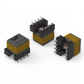
The auxiliary gate drive transformers are an integral part and very important for powering the gate drive circuits of the SiC MOSFETs. Rugged galvanic isolation, compliance with safety standards, control signal noise immunity and EMI performance are just some of the most important aspects to consider. An optimal design of the isolated auxiliary supply providing the voltage and current levels to drive the SiC/GaN device is critical to help the full gate driver system meet the many requirements set by state-of-the-art applications. With the WE-AGDT transformer series, Würth Elektronik addresses the current and future challenges in the field of power electronics and gives engineers the possibility to easily implement a discrete solution of a very compact and efficient gate driver supply with up to 6 W output power. This meets the low interwinding capacitance requirements (sometimes down to 1,5pF) demanded by many modern applications with fast switching SiC/GaN as well as IGBT devices.

Figure 5. WE-AGDT Auxilary Gate Drive Transformer
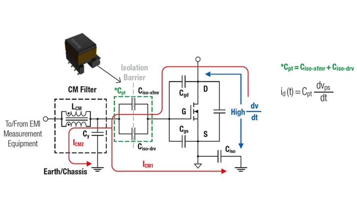
Therefore, high values of Common-Mode Transient Immunity are achieved with this lowering of the interwinding capacitance – higher impedances are seen by the common-mode noise created by displacement current of high dI/dT and dV/dT across the isolation barrier. The result is noise separation of the high voltage side from the low voltage side and therefore smaller EMI filters required on the input. Implementing such auxiliary gate power supplies should be done such that each SiC driving IC has its own power supply, keeping the gate current loop small and local to the device, minimizing the adverse effects of parasitic loop inductance and ground bounce caused by the very high ∆I/∆t generated during the switching transition.

Figure 6. Common-mode currents through isolation barrier
The new PFC inductors with flat wire design are also included in this design. The PFC boost inductors feature flat windings for low DCR and help reduce the skin effect by reducing the height (diameter for a round
conductor) but increasing the surface area (skin), therefore reducing the AC resistance with increasing switching frequencies. From a technical perspective, having flat wire wound in this style with parallel wires and no overlaps, the distributed capacitance is lowered so the inter-winding capacitance is reduced, helping with increasing of the SRF point of the inductor.

Figure 7. Flat wire PFC inductor
To give an idea of the difference that the winding style really has over the inter-winding capacitance, if the same core of the PFC choke is used and a round wire is selected and wound to get the same inductance to the flat wire PFC choke, the measured inter-winding capacitance is around 154 pF for the inductor using round wire. On the other hand, the PFC choke which features flat wire, the measured inter-winding capacitance is just 3 pF. That is 50 times lower just because there are no overlapping layers of wire.

Figure 8. Round wire vs. flat wire winding
DC-link capacitors act as an intermediary DC smoothing stage between AC stages. The intermediate DC step allows noise-reduced power transfer when converting between AC sources of different power, voltage, or frequency conditions. DC-link capacitors are often exposed to high slew rates which can be detrimental if a suitably robust capacitor is not selected. DC-link capacitors are often found in power inverters, motor drives, and high-power charging circuits. Capacitor technologies are sometimes mixed in DC-link applications to target noise and transients that may need multiple stages of filtering.


Figure 9. WE-FTDB DC-Link Capacitors
The DC-Link capacitors were of paramount importance for the PFC stage and a good product is essential for keeping the high voltage DC stable and avoiding losses. The series features self-healing properties, high ripple current capability, polypropylene dielectric and a high voltage range of 500-1200Vdc.
This design provides a compact, ready-to-deploy solution with an optimized BOM and takes control of the latest technology in SiC modules from onsemi. This full SiC solution consists of PFC and DC-DC stages featuring multiple 1200V, 10 mohm half-bridge SiC modules NXH010P120MNF1, the ultralow RDS(ON) and minimized parasitic inductance can significantly reduce conduction loss and switching loss. Relying on the powerful Universal Controller Board (UCB) with Zynq®-7000 SoC FPGA and ARM®-based processor, the system can deliver maximum 25kW over 200V-1000V output voltage with 96% all-time efficiency to charge 400V or 800V EV batteries.
With the support of the Wurth Elektronik IC Support Team and its Product Management for developing products fit for the design and driven by the requirements, we ensured that onsemi had the best-in-class tools for a rugged design. Onsemi‘s market and product requirement knowledge enabled us to develop new series that will fit the market for the years to come in response to the growing SiC trend.

