Support Note
Conducted emissions test
SN023 by Adrian Stirn
01. INTRODUCTION
The conducted emission test is performed according to the test setup defined in the CISPR 16-2-1 standard. This support note discusses the special features of the test setup and the resulting loop impedances.
02. MEASUREMENT METHODOLOGY AND TEST SETUP EMC
test standards aim to reproduce real interference mechanisms in a reproducible manner. However, reproducibility is often more important than the realistic simulation of phenomena. To understand how interference suppression measures work in a targeted manner, these test setups must be understood. With knowledge and rough modeling of the test setup, EMC interference suppression can be calculated to a certain extent.
2.1 Test setup
In the conducted emissions testing, the device under test (DUT) is connected to an artificial mains network (AMN) at the AC power supply connections and to asymmetric artificial network (AAN) at the network connections. Network connections are signal connections that are connected to a network, such as Ethernet or the KNX bus. Point-to-point connections such as USB connections do not fall under the tested interfaces.
CISPR 16-2-1 provides various options for setting up the conducted emissions test. All setups have in common that the coupling networks measure the interference voltage against a common reference ground plane, which is located at a distance of 40 cm from the DUT. Figure 1 shows the test setup through the reference ground plane. The coupling networks are located at a distance of 80 cm from the DUT.
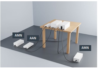
Figure 1: Setup of the conducted disturbance measurement according to CISPR 16-2-1.
Figure 2 shows the relevant distances again in a two-dimensional view. All coupling networks used must be terminated with 50 Ω, either by the impedance of the EMI receiver or by means of an external resistor.
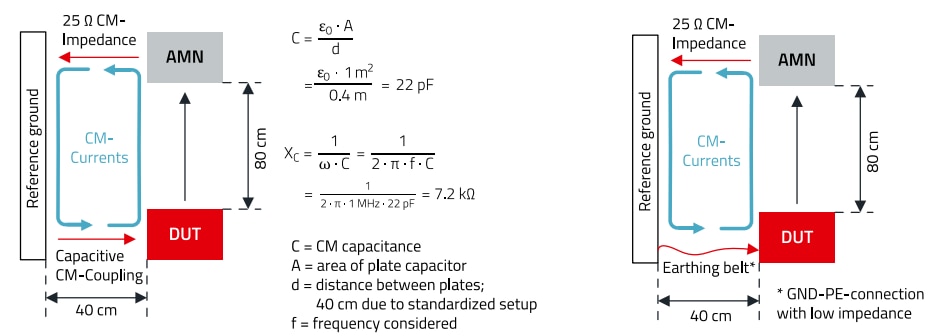
Figure 2: Loop impedance when testing the conducted interference emission.
AANs have an impedance of 150 Ω against the ground plane, AMNs have an S-shaped impedance curve that reaches 50 Ω at approx. 1 MHz (see Figure 3).
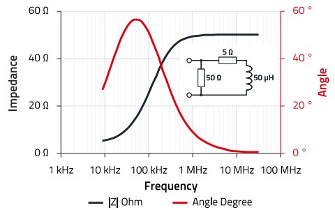
Figure 3: Impedance curve of a 50 Ω / 50 µH + 5 Ω AMN according to CISPR 16-1-2.
The coupling networks measure both common mode and differential mode interferers. It is not possible to differentiate between them from the result of conducted emissions test.
2.2 Loop impedance
If a suitable common mode line filter is to be designed for the DUT, the loop impedances in the test setup must be understood. Figure 2 provides an overview of the impedances in the test setup. To simplify the loop impedances, it is assumed that the coupling network has an impedance of 25 Ω (twice 50 Ω in parallel L + N) for common mode currents. Various cases can occur as coupling between the DUT and the reference ground:
- The DUT has no other interfaces and couples via the stray capacitance. According to the example in Figure 2, this results in a stray capacitance of 22 pF with a coupling area of the DUT of 1 m2. This was derived from the plate capacitor formula.
- The DUT is short-circuited by a functional earth or installation in the chassis of a conductive system. For example: DIN rail device is clicked conductively onto an earthed busbar in the system control cabinet.
- The DUT has shielded network cables that are terminated with a 150 Ω AAN during the emission test. Consideration of the loop impedance shows that the common mode interference currents that lead to the voltage drop across the AMN have strongly varying loop impedances depending on the application. This also means that line filters must be adapted to these conditions.
With an example calculation at an interference frequency of 150 kHz with a coupling capacitance of 22 pF, this results in an impedance of approx. 48 kΩ. If the DUT is connected to the reference ground, this impedance drops to a very low value - the current loop has thus changed significantly. With all these considerations, it must be noted that these are very rough rule of thumb calculations in order to explain and understand the effects during the EMC test. The aim is to select the correct topology and suitable component sizes for the mains filter.
The connection of a secondary device to a DUT is often ignored in the EMC risk assessment of the DUT. For example, a USB interface can be tested with a USB stick. In this case, there is no conductive coupling to the reference ground. However, if a device with a protective earth conductor is connected to the USB port instead of a USB stick, the interface is earthed via the USB shield with a relatively low impedance (rough estimate curve is frequency-dependent). As in the example shown above, the loop impedance changes significantly, and the results of the conducted emissions can change considerably.
2.3 Measurement of common mode and differential mode interferers
As conducted emissions tests produce superimposed measurement results from common and differential mode interference, the interference components must be differentiated in the EMC laboratory before the filter design. Traditionally, an RF current clamp is used for this and the cables are fed through the current clamp as shown in Figure 4.

Figure 4: Measurement of the common mode currents on the left-hand side and the differential mode currents on the right-hand side.
The result on the EMI receiver shows the interference current through both wire pairs as differential mode current and common mode current. Caution: Due to the impedance from the coupling network and partial non-linearity of the current clamp, distortions may occur between interference current and interference voltage. However, the result at the frequency range between differential mode and common mode remains consistent, as the ratio is correct in each case. When measuring with current clamps, it is important that this distinction is made in the impedance system of the conducted emissions test setup. If the measurement is carried out on the laboratory bench, the reference system and thus the coupling impedances of the normative set-up are missing. This changes the common mode currents, and the measurement result deviates from the normative measurement.
03. FILTER DESIGN
Once the setup of the conducted emissions and the resulting impedances are understood and the interference currents are differentiated into common mode and differential mode, a filter can be designed according to the Application Note ANP015. In the following section, the effect of a filter in the overall system is considered using the example of a power supply unit.
3.1 Origin of common mode interferer
Common mode interference mainly occurs in power supply units with galvanic isolation due to the stray capacitance of the transformer. The power electronics switch with fast clock edges and thus generate a rapidly changing voltage (dV / dt). Due to the coupling capacitance between the primary and secondary side, common mode interference is coupled into the system from Figure 2. The interference source is therefore the coupling capacitance of the transformer with a source impedance defined by the coupling capacitance. A common way of reducing common mode interference in the circuit is to use capacitors between the primary and secondary sides of the transformer. Voltage-resistant Y-capacitors are usually used here, whose capacitance should be a factor of 100 higher than the stray capacitance of the transformer according to the rule of thumb. A low stray capacitance of the transformer reduces the capacitance of the capacitors required from the primary to the secondary side, reduces the coupling of the common mode interference current and thus also reduces the overall filter effort. Similar effects must also be taken into account for motor-inverter systems - keyword: motor stray capacitance.
3.2 Capacitive shield plate / chassis
The discussion of the common mode loop impedances in Figure 2 shows that the coupling capacitance is nevertheless small for DUTs with a large surface area, resulting in a very large loop impedance.
Increasing the impedance in the filter is therefore not expedient. Instead, you should try to keep the interference in the power supply unit and create a return current loop via the chassis or a capacitively coupled "shielding". However, if the loop impedance is already very low, for example because a shielded interface cable is connected, increasing the impedance using CMC can reduce the interference very effectively.
Figure 5 shows the filter used with a coupling plate or chassis.
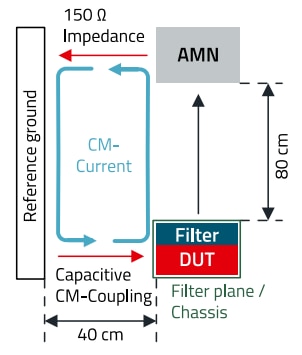
Figure 5: DUT in the overall setup of the conducted emissions test with chassis and filter.
The distance between the coupling plate and the electronic circuits is significantly less than the distance between the 40 cm coupling capacitance to the reference ground. The interference current will therefore flow onto the chassis and is then fed back into the filter via the Y-capacitors. The circuit is thus closed via the filter - the interference current is conducted by passing the coupling network. In the device itself, the interference current increases because the loop impedance decreases - therefore higher interference is to be expected in the device, but the environment is no longer disturbed. To ensure successful interference suppression using EMC filters, the filter components should be designed in accordance with the following design recommendations.
3.3 Placement of the components
As the loop impedance is controlled by the filter, the components should be placed as effectively as possible to avoid crosstalk or additional parasitic effects. Figure 6 shows the important points when setting up a mains filter. The filter components are connected by wires in the picture - this is to make it clear that no conductive surfaces or traces should be drawn under the filter components. This prevents the filter from being overcoupled by the interference. The chassis is shown in gray in the background and below the electronic module. This forms the return current path for the interference currents, which then flow back into the circuit via the directly connected metallic studs via the Y-capacitors. To keep the leakage inductance of the capacitors as low as possible, they should be connected directly to the chassis via the shortest possible route using bolts. With multi-stage filters, each Y-capacitor stage requires its own connecting stud in order to avoid over-coupling of the derived interference from the first pair of capacitors.
The RF leakage current leads to an RF voltage drop in the stud, which in turn would couple into the next stage Y-capacitors. In the direction of the mains, the last common mode choke is always terminated with an X-capacitor in order to short-circuit any differential interference coupled into the common mode choke of the filter by magnetic fields. In addition, differential interference from the electronics is filtered by the leakage inductance of the common mode choke.
Note: Using the chassis as a reference only works if it is also free of interference. If the entire housing, and thus the reference ground, already has a high interference potential, for example because the power semiconductors are screwed on for cooling, the interference can be fed back via the Y-capacitors - a detailed analysis is then required to find a solution.
If a device has more than a mains connection, the filters of the other interfaces may also have to be connected to the chassis and cable shields need to be fully (no pig tail) connected to the chassis.
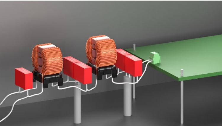
Figure 6: Schematic design of a mains filter. The wired structure can be replaced by FR4 without conductive surfaces or other traces.
IMPORTANT NOTICE
The Application Note is based on our knowledge and experience of typical requirements concerning these areas. It serves as general guidance and should not be construed as a commitment for the suitability for customer applications by Würth Elektronik eiSos GmbH & Co. KG. The information in the Application Note is subject to change without notice. This document and parts thereof must not be reproduced or copied without written permission, and contents thereof must not be imparted to a third party nor be used for any unauthorized purpose. Würth Elektronik eiSos GmbH & Co. KG and its subsidiaries and affiliates (WE) are not liable for application assistance of any kind. Customers may use WE’s assistance and product recommendations for their applications and design. The responsibility for the applicability and use of WE Products in a particular customer design is always solely within the authority of the customer. Due to this fact it is up to the customer to evaluate and investigate, where appropriate, and decide whether the device with the specific product characteristics described in the product specification is valid and suitable for the respective customer application or not. The technical specifications are stated in the current data sheet of the products. Therefore the customers shall use the data sheets and are cautioned to verify that data sheets are current. The current data sheets can be downloaded at www.we-online.com. Customers shall strictly observe any product-specific notes, cautions and warnings. WE reserves the right to make corrections, modifications, enhancements, improvements, and other changes to its products and services. WE DOES NOT WARRANT OR REPRESENT THAT ANY LICENSE, EITHER EXPRESS OR IMPLIED, IS GRANTED UNDER ANY PATENT RIGHT, COPYRIGHT, MASK WORK RIGHT, OR OTHER INTELLECTUAL PROPERTY RIGHT RELATING TO ANY COMBINATION, MACHINE, OR PROCESS IN WHICH WE PRODUCTS OR SERVICES ARE USED. INFORMATION PUBLISHED BY WE REGARDING THIRD-PARTY PRODUCTS OR SERVICES DOES NOT CONSTITUTE A LICENSE FROM WE TO USE SUCH PRODUCTS OR SERVICES OR A WARRANTY OR ENDORSEMENT THEREOF. WE products are not authorized for use in safety-critical applications, or where a failure of the product is reasonably expected to cause severe personal injury or death. Moreover, WE products are neither designed nor intended for use in areas such as military, aerospace, aviation, nuclear control, submarine, transportation (automotive control, train control, ship control), transportation signal, disaster prevention, medical, public information network etc. Customers shall inform WE about the intent of such usage before design-in stage. In certain customer applications requiring a very high level of safety and in which the malfunction or failure of an electronic component could endanger human life or health, customers must ensure that they have all necessary expertise in the safety and regulatory ramifications of their applications. Customers acknowledge and agree that they are solely responsible for all legal, regulatory and safety-related requirements concerning their products and any use of WE products in such safety-critical applications, notwithstanding any applications-related information or support that may be provided by WE. CUSTOMERS SHALL INDEMNIFY WE AGAINST ANY DAMAGES ARISING OUT OF THE USE OF WE PRODUCTS IN SUCH SAFETY-CRITICAL APPLICATIONS.
DIRECT LINK
SN023 | Conducted emissions test
USEFUL LINKS:
Application Notes : https://we-online.com/en/support/knowledge/application-notes
Services: https://we-online.com/en/products/components/service
Contact : https://we-online.com/en/support/contact
CONTACT INFORMATION
Würth Elektronik eiSos GmbH & Co. KG
Max-Eyth-Str. 1, 74638 Waldenburg, Germany
Tel.: +49 (0) 7942 / 945 – 0
Email: appnotes@we-online.de
Web: https://www.we-online.com

