element14 Community
element14 Community
    Register Log In
  • Site
  • Search
  • Log In Register
  • Community Hub
    Community Hub
    • What's New on element14
    • Feedback and Support
    • Benefits of Membership
    • Personal Blogs
    • Members Area
    • Achievement Levels
  • Learn
    Learn
    • Ask an Expert
    • eBooks
    • element14 presents
    • Learning Center
    • Tech Spotlight
    • STEM Academy
    • Webinars, Training and Events
    • Learning Groups
  • Technologies
    Technologies
    • 3D Printing
    • FPGA
    • Industrial Automation
    • Internet of Things
    • Power & Energy
    • Sensors
    • Technology Groups
  • Challenges & Projects
    Challenges & Projects
    • Design Challenges
    • element14 presents Projects
    • Project14
    • Arduino Projects
    • Raspberry Pi Projects
    • Project Groups
  • Products
    Products
    • Arduino
    • Avnet & Tria Boards Community
    • Dev Tools
    • Manufacturers
    • Multicomp Pro
    • Product Groups
    • Raspberry Pi
    • RoadTests & Reviews
  • About Us
    About the element14 Community
  • Store
    Store
    • Visit Your Store
    • Choose another store...
      • Europe
      •  Austria (German)
      •  Belgium (Dutch, French)
      •  Bulgaria (Bulgarian)
      •  Czech Republic (Czech)
      •  Denmark (Danish)
      •  Estonia (Estonian)
      •  Finland (Finnish)
      •  France (French)
      •  Germany (German)
      •  Hungary (Hungarian)
      •  Ireland
      •  Israel
      •  Italy (Italian)
      •  Latvia (Latvian)
      •  
      •  Lithuania (Lithuanian)
      •  Netherlands (Dutch)
      •  Norway (Norwegian)
      •  Poland (Polish)
      •  Portugal (Portuguese)
      •  Romania (Romanian)
      •  Russia (Russian)
      •  Slovakia (Slovak)
      •  Slovenia (Slovenian)
      •  Spain (Spanish)
      •  Sweden (Swedish)
      •  Switzerland(German, French)
      •  Turkey (Turkish)
      •  United Kingdom
      • Asia Pacific
      •  Australia
      •  China
      •  Hong Kong
      •  India
      •  Japan
      •  Korea (Korean)
      •  Malaysia
      •  New Zealand
      •  Philippines
      •  Singapore
      •  Taiwan
      •  Thailand (Thai)
      •  Vietnam
      • Americas
      •  Brazil (Portuguese)
      •  Canada
      •  Mexico (Spanish)
      •  United States
      Can't find the country/region you're looking for? Visit our export site or find a local distributor.
  • Translate
  • Profile
  • Settings
PCB Design, Prototyping and Production
  • Products
  • More
PCB Design, Prototyping and Production
PCB Blogs PCB Art:  The Scream
  • Blog
  • Forum
  • Documents
  • Leaderboard
  • Files
  • Members
  • Mentions
  • Sub-Groups
  • Tags
  • More
  • Cancel
  • New
Join PCB Design, Prototyping and Production to participate - click to join for free!
  • Share
  • More
  • Cancel
Group Actions
  • Group RSS
  • More
  • Cancel
Engagement
  • Author Author: fmilburn
  • Date Created: 24 Jan 2020 3:07 AM Date Created
  • Views 3537 views
  • Likes 13 likes
  • Comments 19 comments
  • pcb_art
  • kicad
  • photoshop
  • pcb
  • art
Related
Recommended

PCB Art:  The Scream

fmilburn
fmilburn
24 Jan 2020

I decided to give PCB art a try and will be basing my attempt on methods described by Andrew Sowa.  Andrew uses Adobe Illustrator for the art work and KiCad for the PCB design.  I will also use KiCad but will use my trusty pre-subscription version of Photoshop for the artwork.  Inkscape is another possibility.  Andrew's process is described in this video from which my work is derived.  The detail behind many of the steps won't be described in this post - watch the video for that.


The goal is to take a photograph, painting, etc. and place it on a PCB using the FR4, copper layer, solder mask, and silk screen to make the palette.  My PCB will feature the famous work by Edvard Munch, The Scream which has always fascinated me.  So, how to turn a masterpiece into a PCB facsimile?image


Palette


The limited palette is a challenge.  For this exercise the focus will be on the central figure in order to reduce board size (and thus cost) of the experiment.  The OSHPark purple solder mask will hopefully give the dark colors desired.  Andrew also used OSHPark in his example, and helpfully provided a palette which has been modified here to help describe how the layers translate to color and are stacked for conversion in KiCad.

image

Different colors will be obtained for different layer transparencies and tints from other board houses.


Photoshop Workflow


The five colors in the palette must be separated into different layers in the software of choice.  My workflow in Photoshop is as follows:

  1. Create a B&W layer
  2. Create a working layer from the background / B&W layer
  3. Using the Magic Wand Tool (adjust tolerance as needed) select the darkest layer (#5 in the palette) from the working layer
  4. Create a new layer using only the selected area and give it a name (e.g. #5_Mask_on_bare for the darkest layer)
  5. Select the current color (#5 for the darkest layer) from the color picker or palette above and fill the selected area with the color
  6. Delete the selected area from the working layer
  7. Repeat steps 3 - 6 above for the next lighter area until all colors in the palette are selected and all areas of the image are filled with colors from the palette.


When these steps are completed the individual layers in Photoshop look something like this:

{gallery} Photoshop Layers

image

Silk Layer

image

Copper Layer

image

Bare FR4 Layer

image

Mask on Copper Layer

image

Mask on bare FR4 Layer


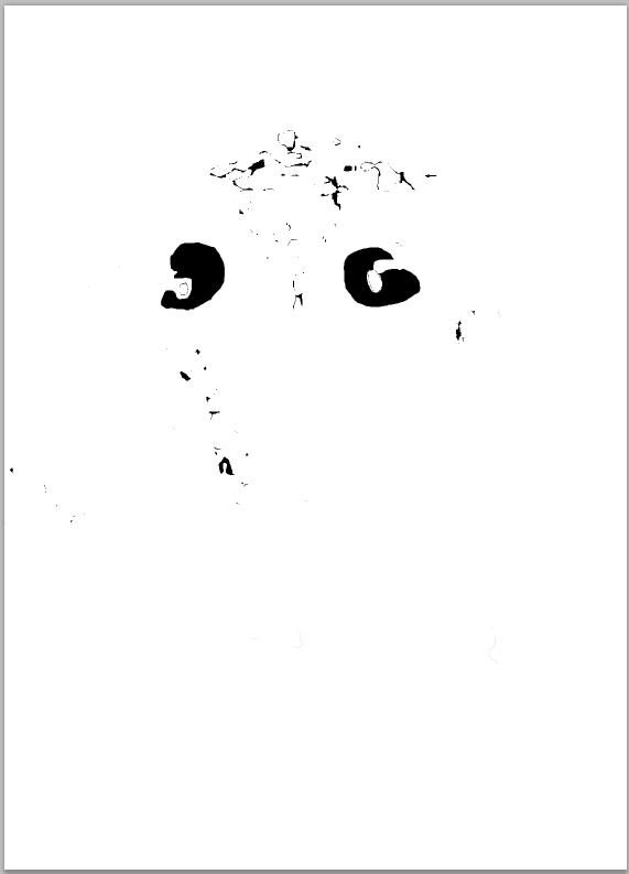
The full image with all layers showing as it appears in Photoshop is shown below.

image


Next prepare the layers that will be used in KiCad.  The layers are copper (both bare and covered by other layers), mask, and silk.  To do this, combine the layers as shown at the bottom of the palette and convert them to a B&W image.   I used png file format set to 400 DPI and roughly the size I wanted (1 x 1.5 inches).  The resulting images are shown below.


{gallery} Layer Images Converted for KiCad

REPLACE THIS TEXT WITH YOUR IMAGEimage

Silk

image

Mask

image

Copper

The work flow in Illustrator demonstrated by Andrew is much different and judging from the video has advantages.  However, my method proved quite workable.


KiCad Conversion Workflow


From this point on everything is the same as in Andrew's video.  KiCad has a learning curve and the details are beyond the scope of this post.  But here it is in outline form...


  • Pull the three B&W images from the last step one at a time into the KiCad Bitmap to Component Converter.
  • Adjust resolution if necessary but not much higher than 400 DPI
  • Set the radio button to Pcbnew (.kicad_mod file)
  • Set Black / White Threshold to 63
  • Set Board Layer for Outline as follows:
    • Front silk screen for silk screen layer
    • Front solder mask for mask and copper layers
  • Export someplace it can be found with meaningful names like Silk, Copper, and Mask


The conversion panel will look something like this:

image


If named as I did there will be three resultant files:  Copper.kicad_mod, Mask.kicad_mod, and Silk.kicad_mod.  Follow the following steps:

  • Copy the file named Silk to a new file which will be combined with the mask and copper ones to make a footprint in KiCad (I named my file scream.kicad_mod)
  • Open up the Mask.kicad_mod file and copy all sections with fp_poly in the leader to just below the last closing parenthesis ")" in the combined file.  Don't copy the header with fp_text and don't copy the closing parenthesis in the Mask file.
  • Open up the Copper.kicad_mod file in Notepad++ or other text editor and replace all instances of Mask with Cu
  • Copy all sections of Copper.kicad_mod with fp_poly in the leader to just below the last closing parenthesis ")" in the combined file of Copper.kicad_mod.  Don't copy the header with fp_text and don't copy the closing parenthesis in the Copper file.


There will now be a combined file which can be used to create a footprint in KiCad which has the layers defined in the 5 colors of the palette.


KiCad Pcbnew Workflow


Inside of Pcbnew, open up the footprint editor and from the File pulldown select Import Footprint from KiCad file... Navigate to the location of the combined file (in this case the file scream.kicad_mod) and select it.  The footprint will appear as shown below:

image

If desired, view it in the 3D Viewer to make sure it looks right.  Save it in the appropriate library.


Now select the Add Footprints tool and place the newly generated footprint in the work area.  Layers can be turned off and on to make sure things look correct.  Draw the boundaries of the PCB on the Edge.Cuts layer.  The 3D viewer in KiCad renders it like this:

image

Finally, use Plot to create the gerber files and it is ready to go to the board house.  Below is what the render from OSHPark looks like.

image

Summary


I won't know how good it really looks until the boards come back but for now I am holding off sending it in.  The primary reason is I would like to add an actual circuit to it. It would be possible to build a simple single layer board with the art on the opposite side but it would be nice if the components somehow enhanced the art.


The process may seem complicated but it took longer to document than it did to figure out how to create the PCB.  Hopefully by documenting the process it will be even quicker next time.  Thanks for reading.  Comments and suggestions are always welcome!


Other posts in this Series


PCB Art:  Screaming LM386

Screaming LM386:  An Audio Amplifier with PCB Art

  • Sign in to reply

Top Comments

  • jw0752
    jw0752 over 6 years ago +5
    Hi Frank, It seems to me that inside every electronics engineer there is a frustrated, or maybe not so frustrated, artist. My attempts have always been very frustrated but I do believe you have a winner…
  • Fred27
    Fred27 over 6 years ago +5
    Some very nice work. It'll be interesting to see how the physical board looks when you get it back. I've been tempted at times to do a PCB business card. One of the things that has held me back is the…
  • Andrew J
    Andrew J over 6 years ago +4
    Brilliant! I’d never even considered the possibility of this, even seeing that people put logos and other images on their boards. I suppose it takes an artist to think of these things... I do like the…
  • Andrew J
    Andrew J over 6 years ago in reply to dubbie

    I bet there are lots of us who want to be experts at a lot of other things!  Maybe it’s an engineer thing.


    B&Q in the UK will only cut wood of a certain length, which is quite long actually, but ‘helpfully’ they will lend you a saw so you can get it into the car image


    Perhaps get some scrap wood and practice on that first.  When I had to cut a rectangle in a piece of aluminium that I didn’t want to otherwise mess up (no replacement!) I went and bought a cheap piece - £2 or £3 and practiced drilling, cutting and filing a rectangle.  It was a bit boring truth be told but when it came to doing it on the actual piece then I was a lot more confident.  By practicing first I also worked out some tips and techniques to make it easier, as well as working out that I needed more appropriate tools.  I’m probably teaching you to suck eggs here, sorry.


    I don’t know where you live but B&Q in Milton Keynes has a ‘scrap’ box by the tills where for an arbitrary donation to a local charity you can take bits of scrap.  I’ve had a number of useful bits of MDF from there.  There might be something similar near to you - that makes it cheap to saw wonky lines until you can saw them straight!  And practicing making the runners parallel.  There we go, teaching you to suck eggs again!!

    • Cancel
    • Vote Up +3 Vote Down
    • Sign in to reply
    • More
    • Cancel
  • 14rhb
    14rhb over 6 years ago in reply to dubbie

    Hi Dubbie,


    Is your mitre saw a powered one or a hand version like this below? The hand ones can have a lot of play in them. especially if they are a low-cost version. Regardless of which perhaps you can adjust them somehow for a better 90 degree cross cut. My low-cost pillar drill is very sloppy but I pulled the chuck back to the main pillar using some medium-springs and was then able to drill out a PCB using 0.3mm drills ! A medium priced electric chop saw however is IMO a great investment - if in the UK have a look at Screwfix or Toolstation websites.


    image

    Regarding your draw unit - IMO MDF isn't very nice for furniture especially if the cut ends are on show. It is OK for the carcass/sides etc but better if edged with some proper wood that can take a knock, have a few dents, get filled, painted or stained. You might find you can buy a cheap plain softwood unit and modify that  - a carboot sale or big DIY chain/Ikea might be useful?


    But being electronics I think it needs a microswitch on the draw and some colour cahnging LEDs inside, at the very least image

    • Cancel
    • Vote Up +3 Vote Down
    • Sign in to reply
    • More
    • Cancel
  • dubbie
    dubbie over 6 years ago in reply to genebren

    Gene,


    I quite agree. I have just moved by daughters old desk from her room to mine. The desk part is very solid but the two draw units seem to be made from cardboard and plastic bags they are so rubbish. It seems surprising that on such a good desk the draws are so poor and have a quite small available space considering their external dimensions. So I am mulling over the idea of making my won stronger draw units with a larger internal space volume. Drawbacks are matching the colour to the desk top, getting the draw runners to be perfectly parallel and my complete inability to saw a straight line in a piece of wood. I have a mitre saw that I could use but even that doesn't (yet anyway) cut at exactly 90 degree angles. I wonder if the local DIY store would cut the pieces I want if I purchased the MDF from them. I've had large shelves cut this way which worked wonderfully, but this might be a larger number of smaller parts. I can only ask and see what they say.


    Dubbie

    • Cancel
    • Vote Up +3 Vote Down
    • Sign in to reply
    • More
    • Cancel
  • 14rhb
    14rhb over 6 years ago

    Hi Frank,


    A great tutorial, thanks for posting this. There seems to be lots of steps (as with any interesting technique) and I'm looking out for your finished boards now image

    • Cancel
    • Vote Up +3 Vote Down
    • Sign in to reply
    • More
    • Cancel
  • fmilburn
    fmilburn over 6 years ago in reply to genebren

    Fully agree.  I have so many interests and don’t stay focused on any one thing long enough to become really expert.

    • Cancel
    • Vote Up +2 Vote Down
    • Sign in to reply
    • More
    • Cancel
<>
element14 Community

element14 is the first online community specifically for engineers. Connect with your peers and get expert answers to your questions.

  • Members
  • Learn
  • Technologies
  • Challenges & Projects
  • Products
  • Store
  • About Us
  • Feedback & Support
  • FAQs
  • Terms of Use
  • Privacy Policy
  • Legal and Copyright Notices
  • Sitemap
  • Cookies

An Avnet Company © 2026 Premier Farnell Limited. All Rights Reserved.

Premier Farnell Ltd, registered in England and Wales (no 00876412), registered office: Farnell House, Forge Lane, Leeds LS12 2NE.

ICP 备案号 10220084.

Follow element14

  • X
  • Facebook
  • linkedin
  • YouTube