Note 1: For a video quick-start guide click here. You can also find some screenshots of configuration windows within KiCad there.
Note 2: Please contribute to this discussion if you can : ) It was started during December 2021, to see if it was possible to learn KiCAD version 6.0.0 and be happy with it. With the help of everyone involved so far, the information below currently discusses how to get up to speed, to be familiar (at a usable level) with the main features of KiCAD (e.g. Preferences, Schematic Editor, Symbol and Footprint Editors, PCB Editor, Plots), from circuit entry through to final Gerber files. The information was tested by trying it out with the creation of a real circuit board.
Table of Contents
Day 1 - Getting familiarized with the Schematic Editor
I've spent several hours today with the new KiCAD version 6.0, in an attempt to see if I can move off an ancient version of EAGLE.
I have tried to use KiCAD once or twice in the past, but always felt uncomfortable and aborted. Today I've got further.
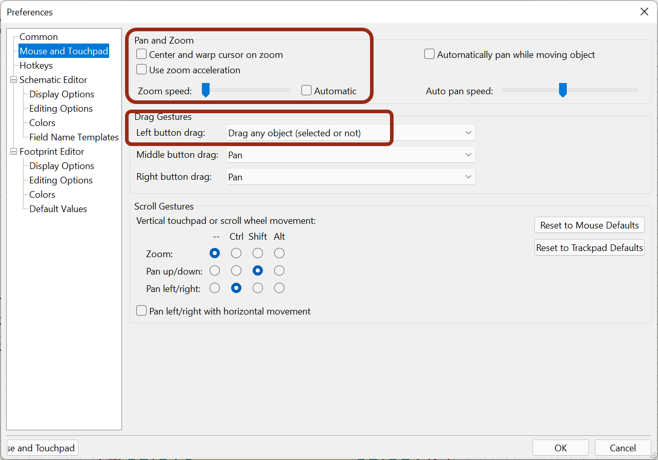
After installing KiCAD, I had to make some preference adjustments (click on Preferences->Preferences in the schematic editor), in order to get the control to something like what EAGLE offered. For me the most important were those highlighted in red below. With these settings as shown in the screenshot, the mouse control felt better.
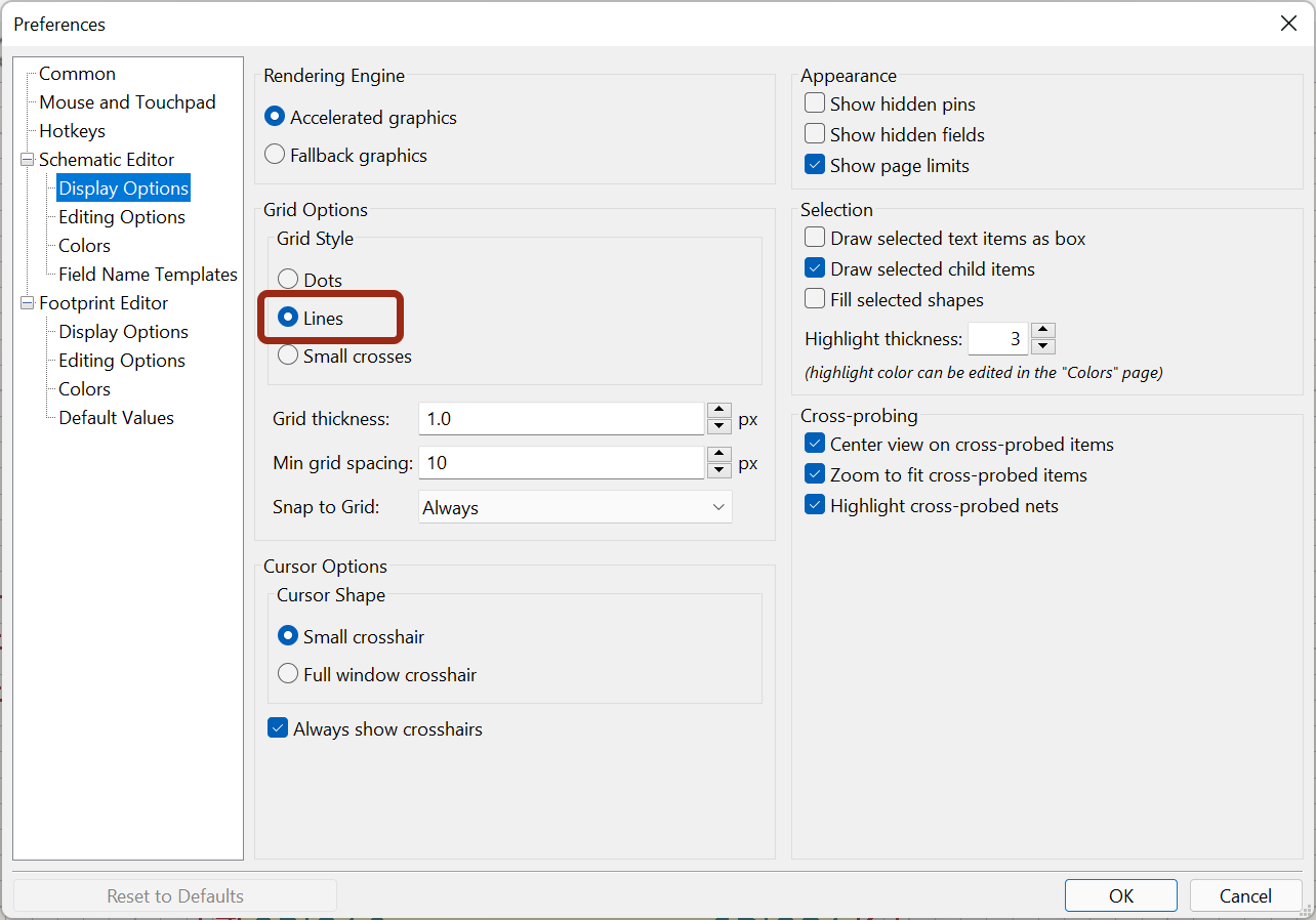
I also changed the grid options to the following:
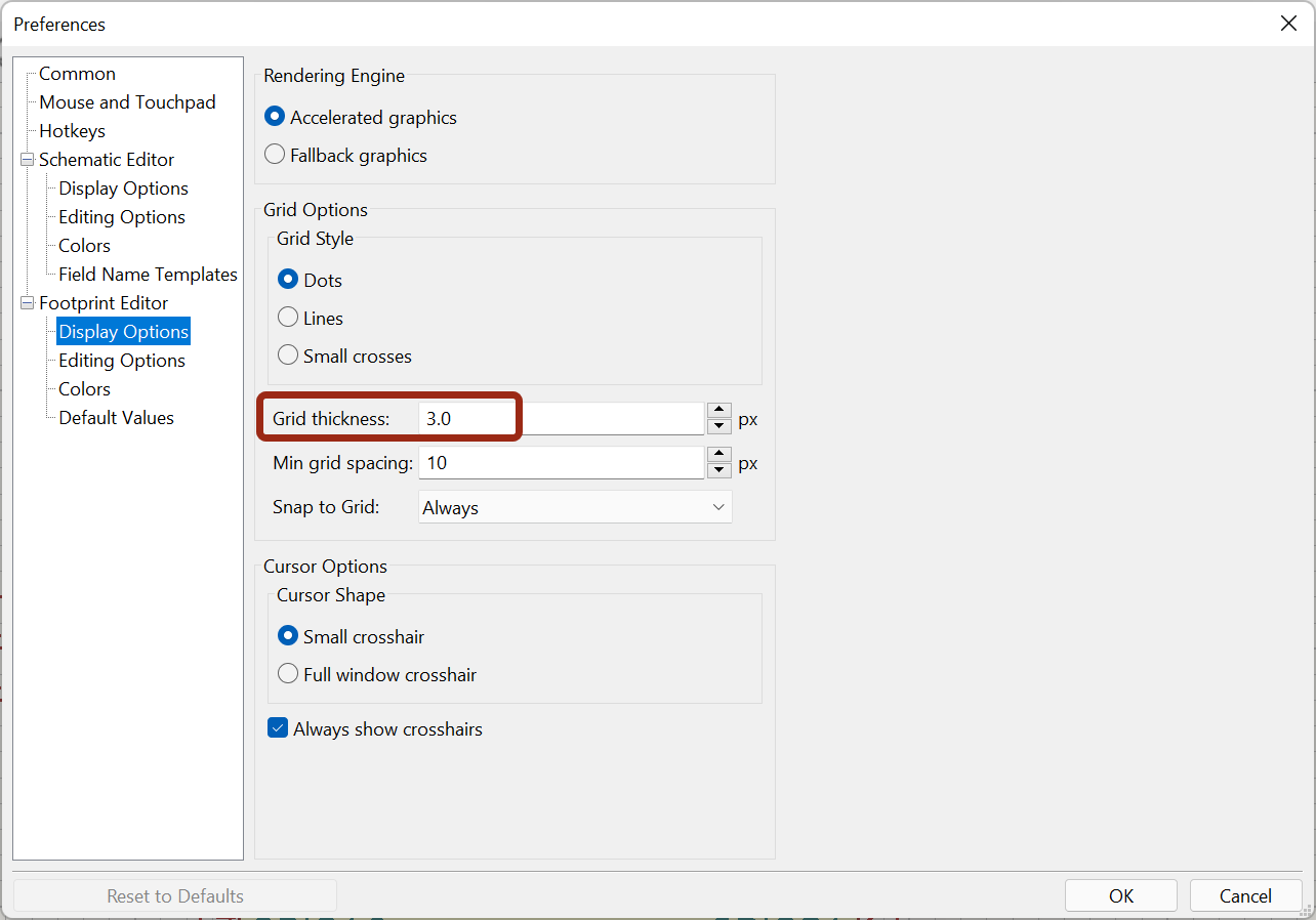
The grid for footprint editing also needed changing (for me):
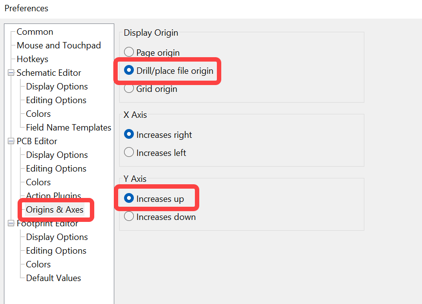
Also, the following is quite important, particularly the Display Origin. Without the Display Origin set as shown in the red box in the screenshot below, when it comes to PCB layout, you won't be able to have the corner of your board (or the center of your board, depending on your preference) at an origin point easily. With the setting as shown below, you can move the origin when you're doing the PCB layout using the Place->Drill/Place File Origin menu option
The Y Axis setting below is only useful if you want your y-co-ordinate values to increase as you go up the page in the PCB editor, which is how it works in EAGLE.:
Now things feel much better!
I have not tried laying out a PCB yet, but have just explored schematic creation, and editing symbols and footprints.
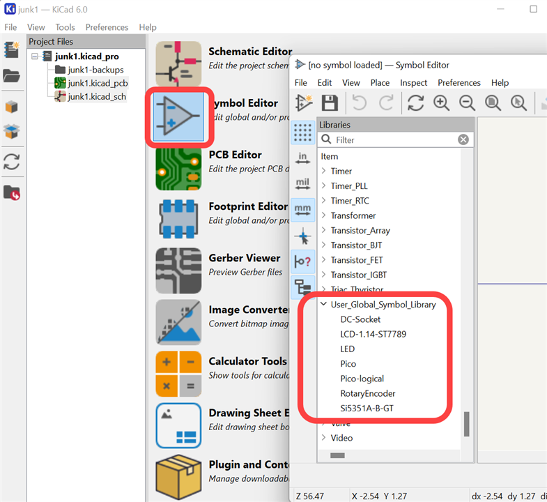
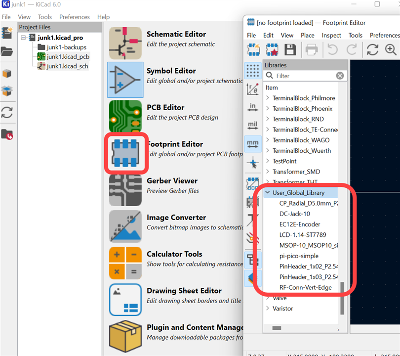
From my perspective, the way I'm working so far is to create my own symbol and footprint libraries (they are separate in KiCAD, whereas in EAGLE it is all in one library file), and then do 'Save As' to save existing symbols or footprints to my own library, whenever I feel the need to edit a symbol or footprint from any source library. I am using 'Global Libraries' (there is an option to have project specific libraries).
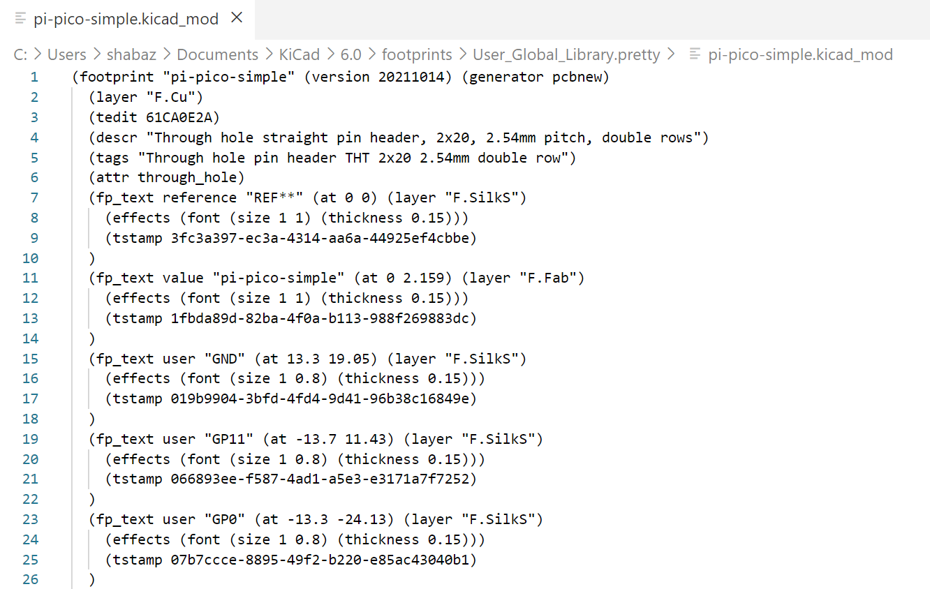
For instance, I needed a Pi Pico symbol and footprint, and found them online (not ventured into creating my own symbols and footprints with KiCAD yet on day 1,but did it later, see further below).
Then, I edited them, and did 'Save As' to save to my own library which I named User Global Library for now. A tidier scheme would be different libraries, but I might over time just add my personal popular symbols into this single library. Unless it grows hugely, I'm assuming it doesn't matter too much because it is easy to find items since there is a search box when you add components or footprints.
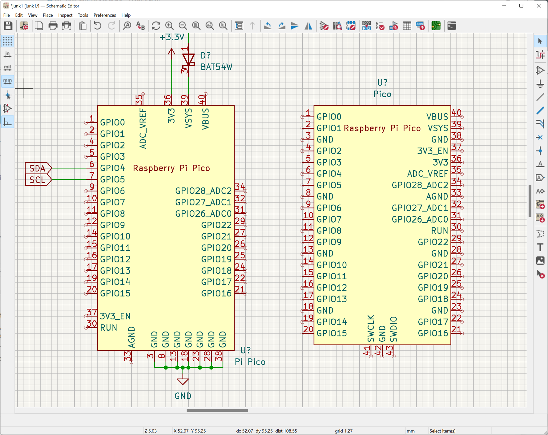
The screenshot below shows the schematic editor with my modified Pi Pico symbol on the left, versus the downloaded one on the right. It could be improved further by collapsing all the GND pins into a single one, but I still need to learn how to do that. For now, I'm happy with the symbol.
Unlike EAGLE, component references (like R1, R2 etc) are not automatically numbered, you have to go to Tools->Annotate Schematic and then click OK, and it will auto-annotate. I don't know of a way to make it automatically annotate in real-time.
After some playing around with the color schemes (you can create your own themes and revert back to the default at any time - this is all from the Preferences menu):
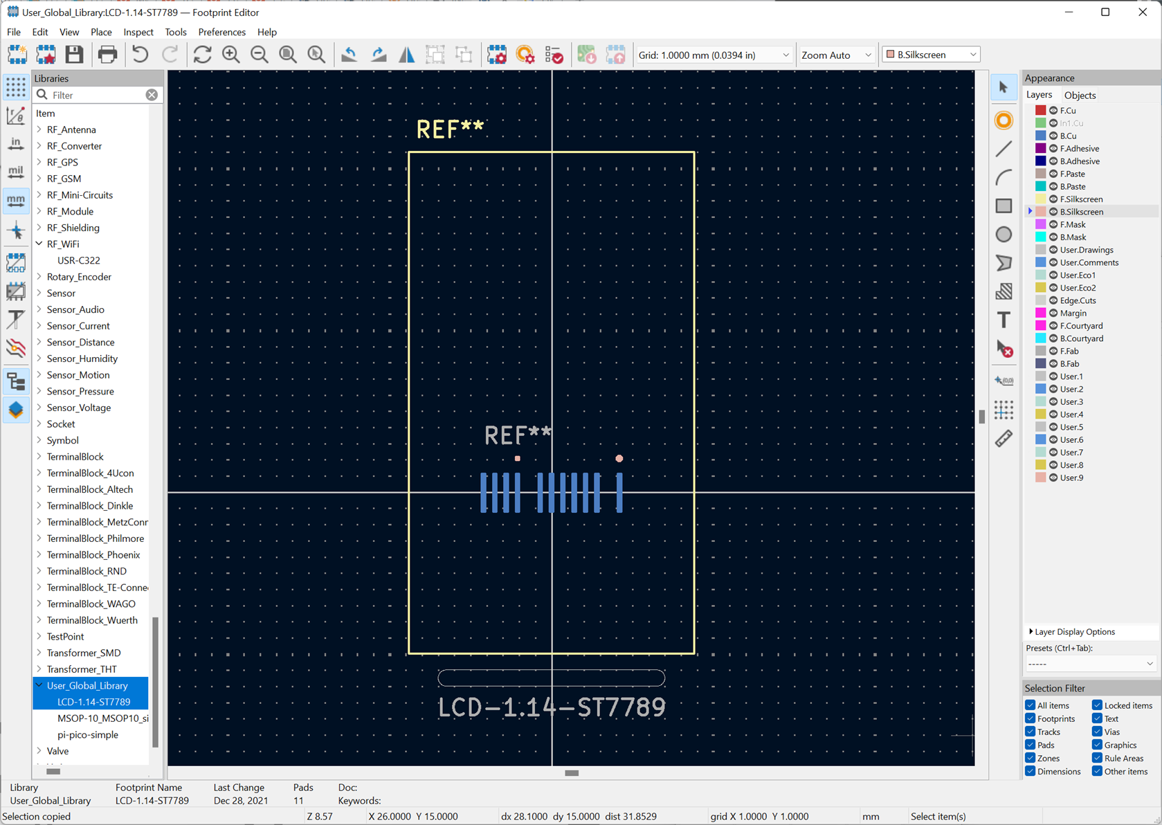
This is what the Footprint Editor looks like:
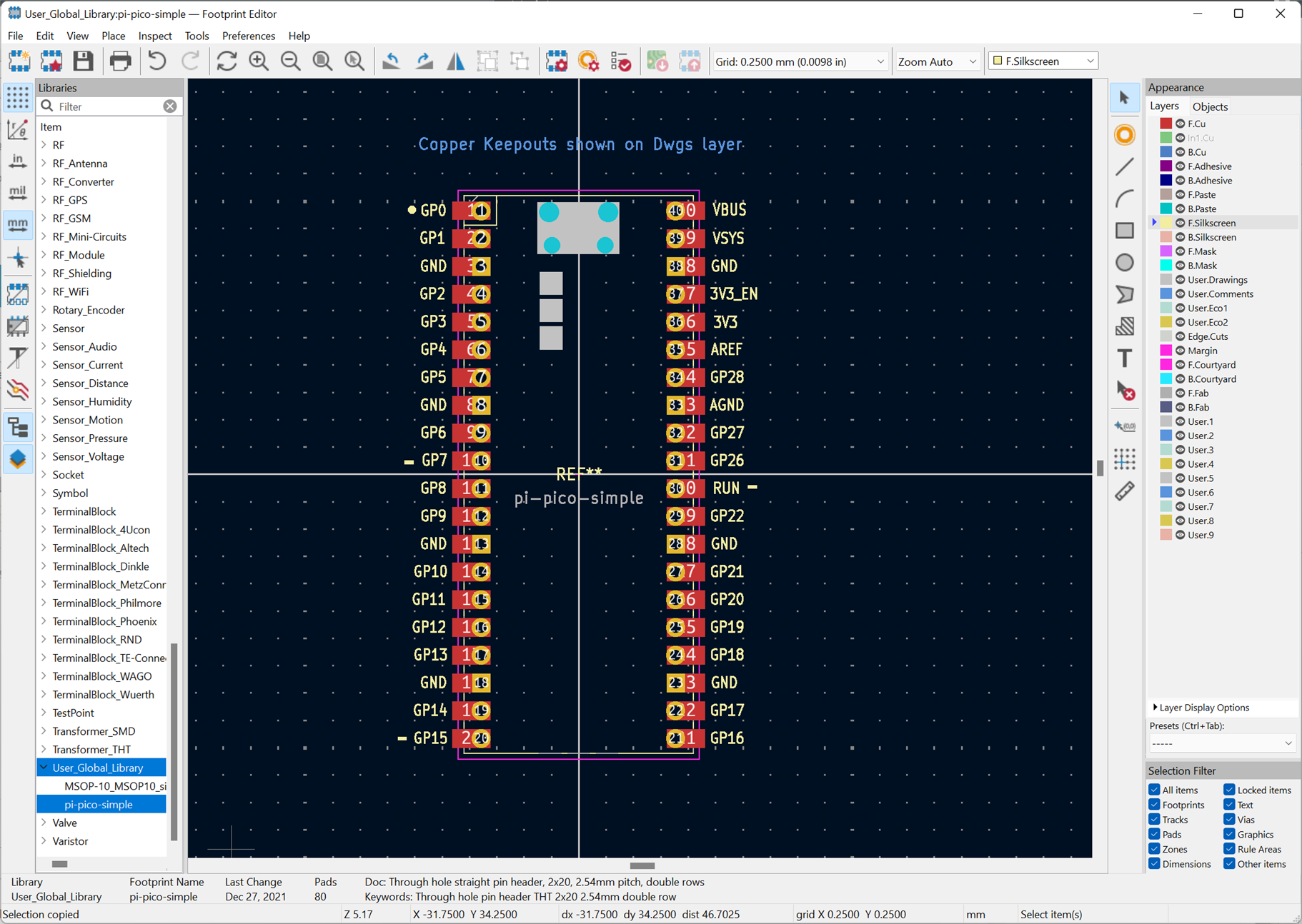
I'm surprised that the footprint editor feels quite nice to use, I was initially dreading it. In some ways it is way more comprehensive than EAGLE (at least the old version I was using!) and in some ways it is missing some functionality, like I couldn't find a way to change the text size in a group.. I had to edit each yellow item of text individually, which took ages. I guess I could have edited the footprint file (unlike EAGLE, each footprint and symbol is in a separate file within each library folder), it's in a strange format but at least it is text-based. Wish it was JSON format.
Anyway, I'm going to continue to take baby steps and see how it goes!
To summarize, KiCAD feels nice to use so far. If the rest of KiCAD is going to be as smooth, then I'm going to be extremely happy about it all!.
Day 3 - Completed Schematic, and did custom Symbols and Footprints
I got a lot further in days two and three, and have completed a full schematic entry, and along the way created a couple of parts (footprint and symbols), as well as edited a few footprints/symbols too.
Throughout, what I've been doing (I don't know if this is best practice or not) is that whenever I see a symbol or footprint that I'd like to tweak, I right-click, Save As and then save it to my User library with either the same name or a different name, and then edit it there. So, now my User libraries for symbols and footprints now look like this after one schematic entry:
During schematic entry, I mostly assigned footprints as I added each component, so that then I could copy-paste from the schematic and know that everything had a footprint assigned. But later I discovered Tools->Assign Footprints which works like this:
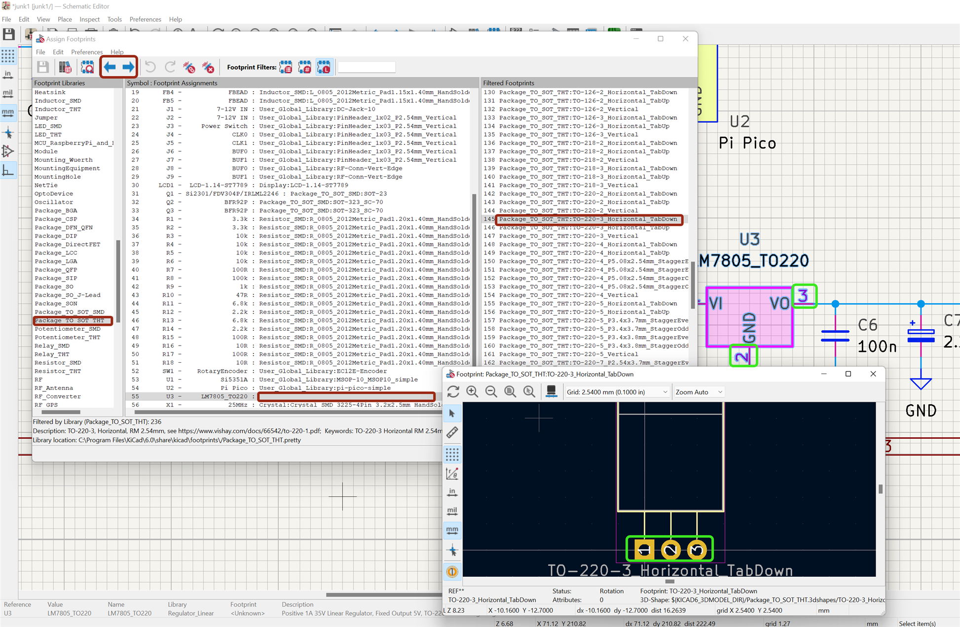
The right/left arrows at the top of the screenshot above are used to navigate through any components that are missing assignments, and then the three columns are used to pick the footprint library and the specific desired footprint. Right-clicking on the footprint name allows you to bring up a graphic view of it.
In EAGLE, there was a mapping table that the user had to fill in to map footprint pad numbers to symbol pin numbers. It seems there is no such table for mapping like this in KiCAD Anyway, I'm happy either way, it is one less step if there is no need for a mapping table.
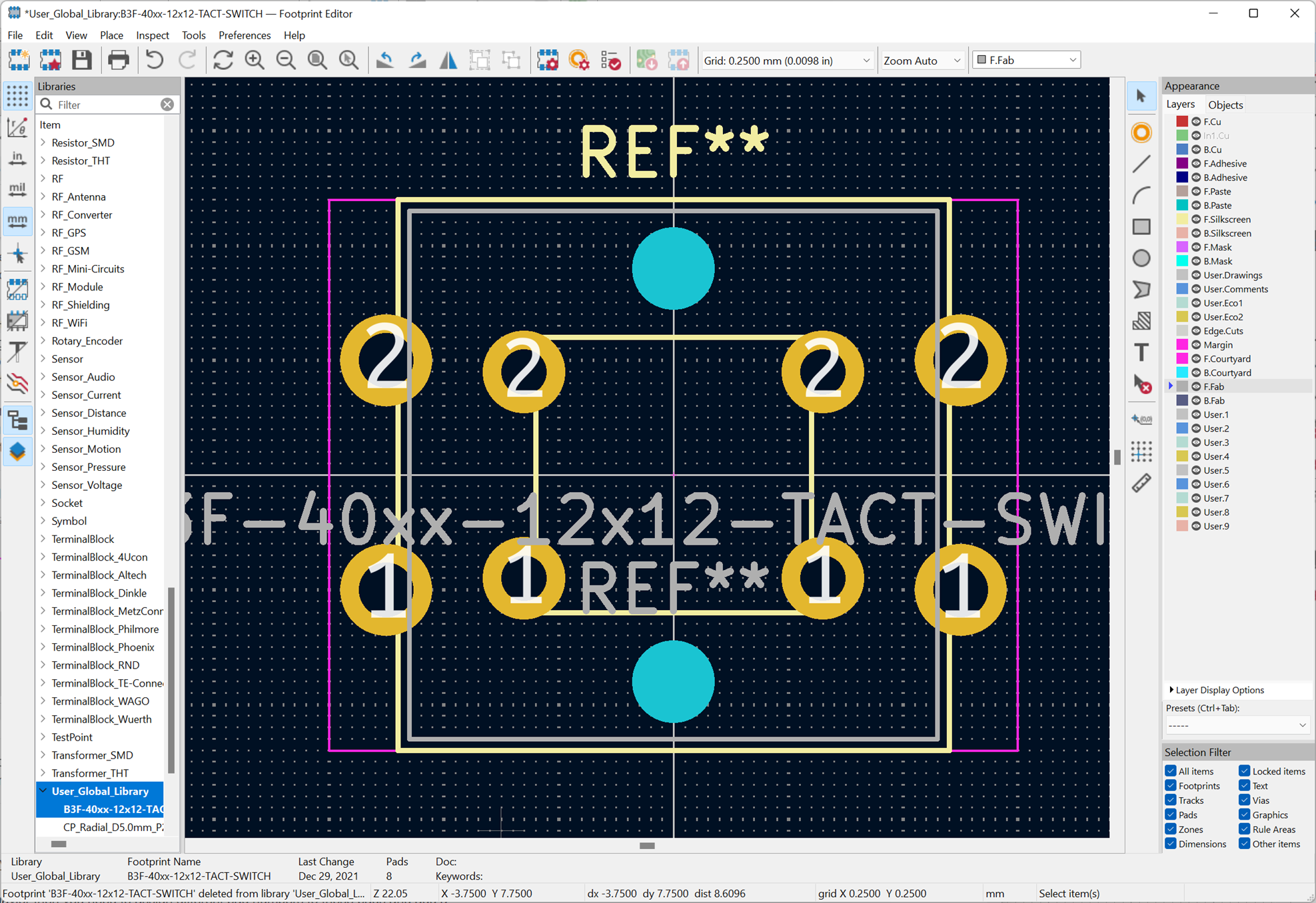
It appears that as shown in the green areas in the screenshot above, the connection pin named 1 on the symbol automatically associates to the pad numbered 1 on the footprint, and so forth for all the remaining numbered pins and pads. If you want lots of pads on the footprint to all to connect to a single pin on the schematic, then just number all those pads with the same value. For instance, here a tactile switch footprint I created with 8 through-hole pads, but they are all just numbered 1 or 2 since the switch symbol will only have two connections. This is less flexible than EAGLE, but I really don't mind in this particular area - I might come to prefer this KiCAD method over time:
By the end of day three, I had a schematic complete, and all symbols have assigned footprints.
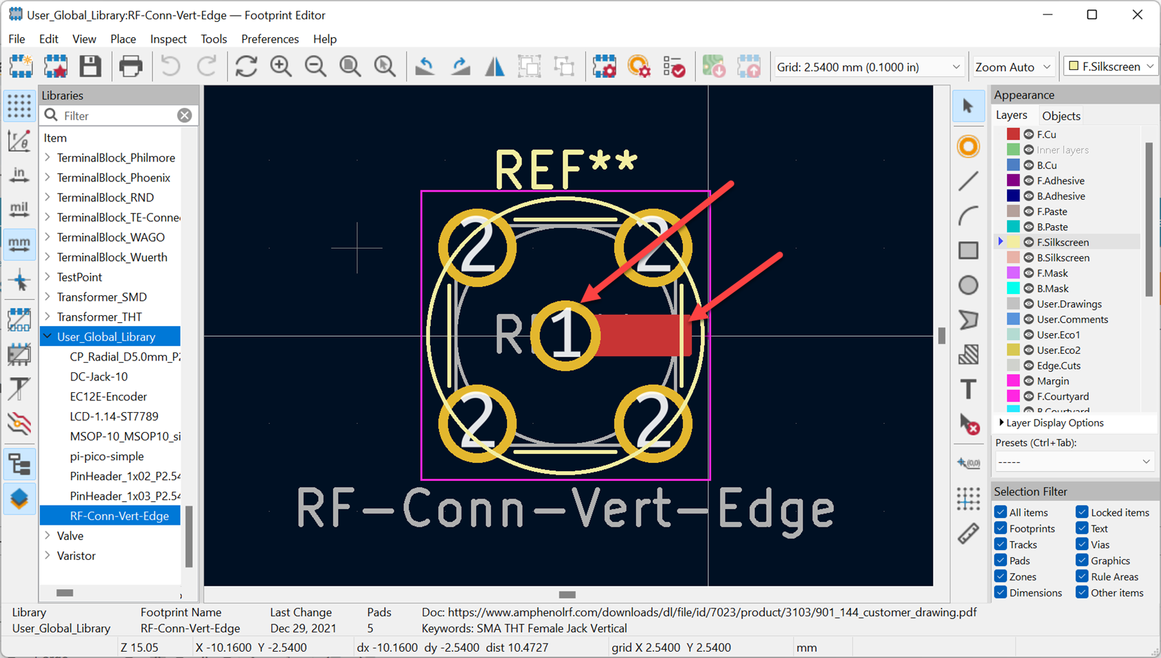
Incidentally, I needed a shaped pad for one of the components, and I just drew a rectangle set to 'filled' overlapping a through-hole pad. I don't know if this is correct, I'll soon find out! (The built-in Footprint Checker at Inspect->Footprint Checker didn't think there was an issue with it). EDIT: I subsequently found out that this didn't work, when it came to routing traces; I couldn't add a trace on top of the rectangle. I don't know why. Anyway, the fix was to delete the red rectangle in the screenshot below, and replace with a SMD pad, set to the same pad number as the through-hole pad. SMD pads are added by clicking on the circular through-hole icon, and then double-clicking it to bring up the properties, and change one of those settings to indicate that it should be a pad.
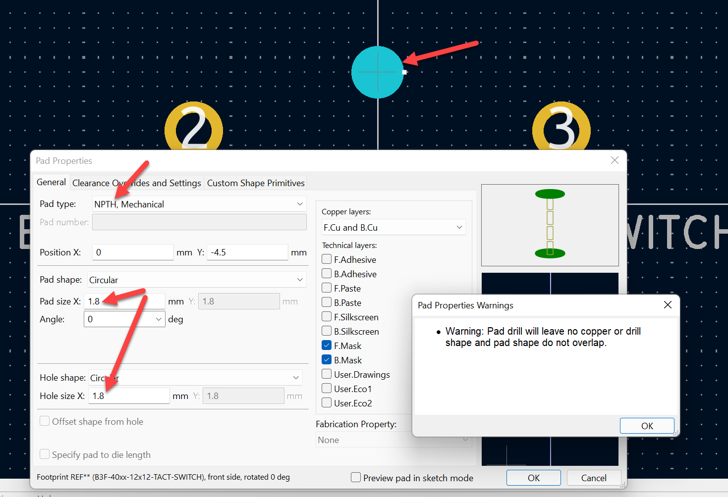
I also need to make a drilled hole (i.e. no pad) in the component footprint, which in KiCAD apparently is done by placing a pad and then changing some attributes as shown here; it does generate a warning box though!:
I managed to make KiCAD crash once : ( I don't know what caused it, but apart from that it's been fine over the three days. EAGLE occasionally crashes too, so I'm not drawing any conclusions from that yet. Anyway, I had happened to have saved quite regularly, so I didn't lose anything. EDIT: I subsequently made KiCAD crash when I ran the Electrical Rule Check (ERC) from the schematic Inspect->Electrical Rules Checker menu item, and raised a bug report (see comments below). The response was quick (within an hour!), and the issue has been assigned to be fixed in the next dot-release. See the comments below to see what to do if there is ever a situation where work is lost (KiCAD archives everything to zip files from time to time automatically in the background, so you can manually revert back to earlier versions if ever required).
Day 4 - PCB Work
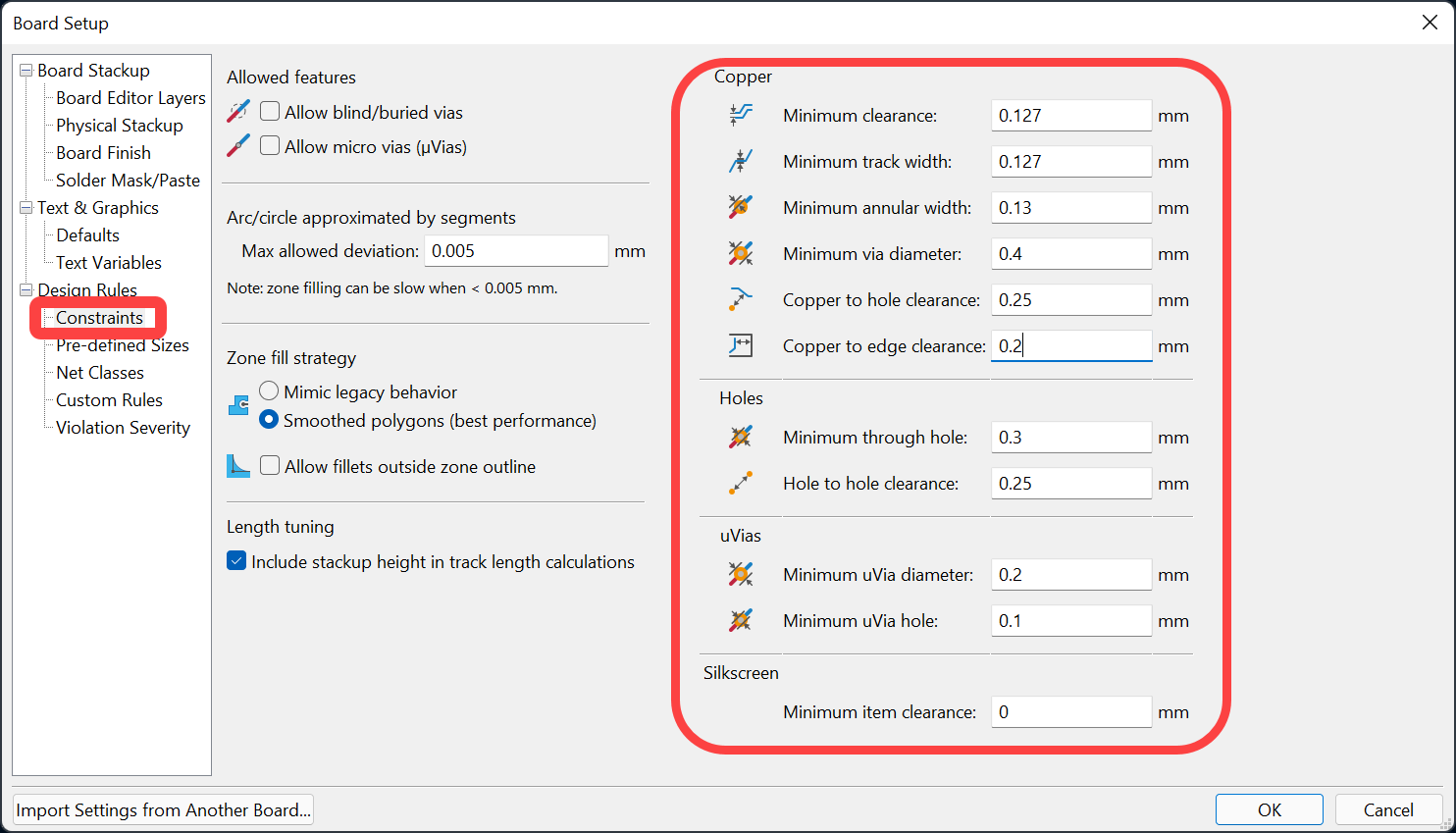
Into day 4, I clicked on the green icon at the top of the Schematic window, to launch the PCB editor. From there, I went to File->Board Setup, went to the Design Rules/Constraints section there, and tried to put in some worst-case limits for basic 2-layer technology. The settings I used are shown in the screenshot here:
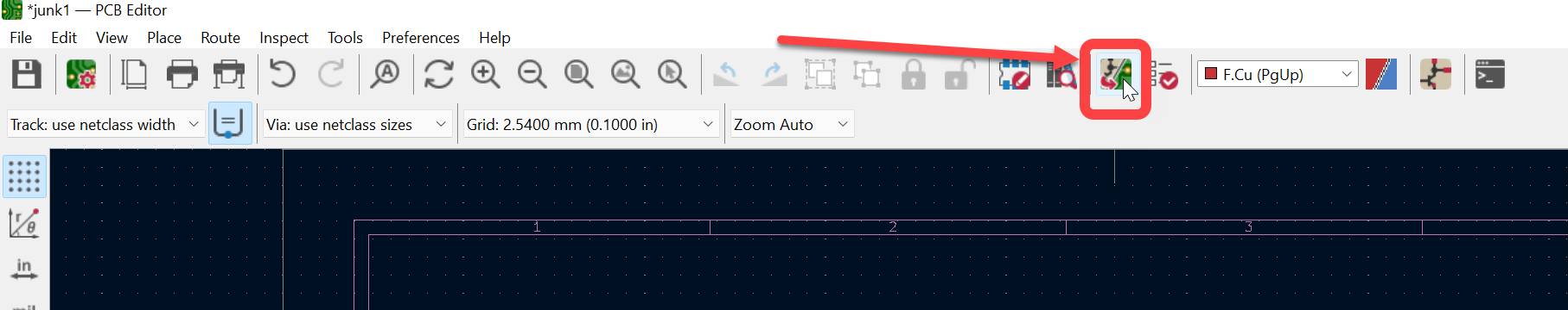
Next, I clicked on the Update PCB with changes made to the Schematic icon as shown here:
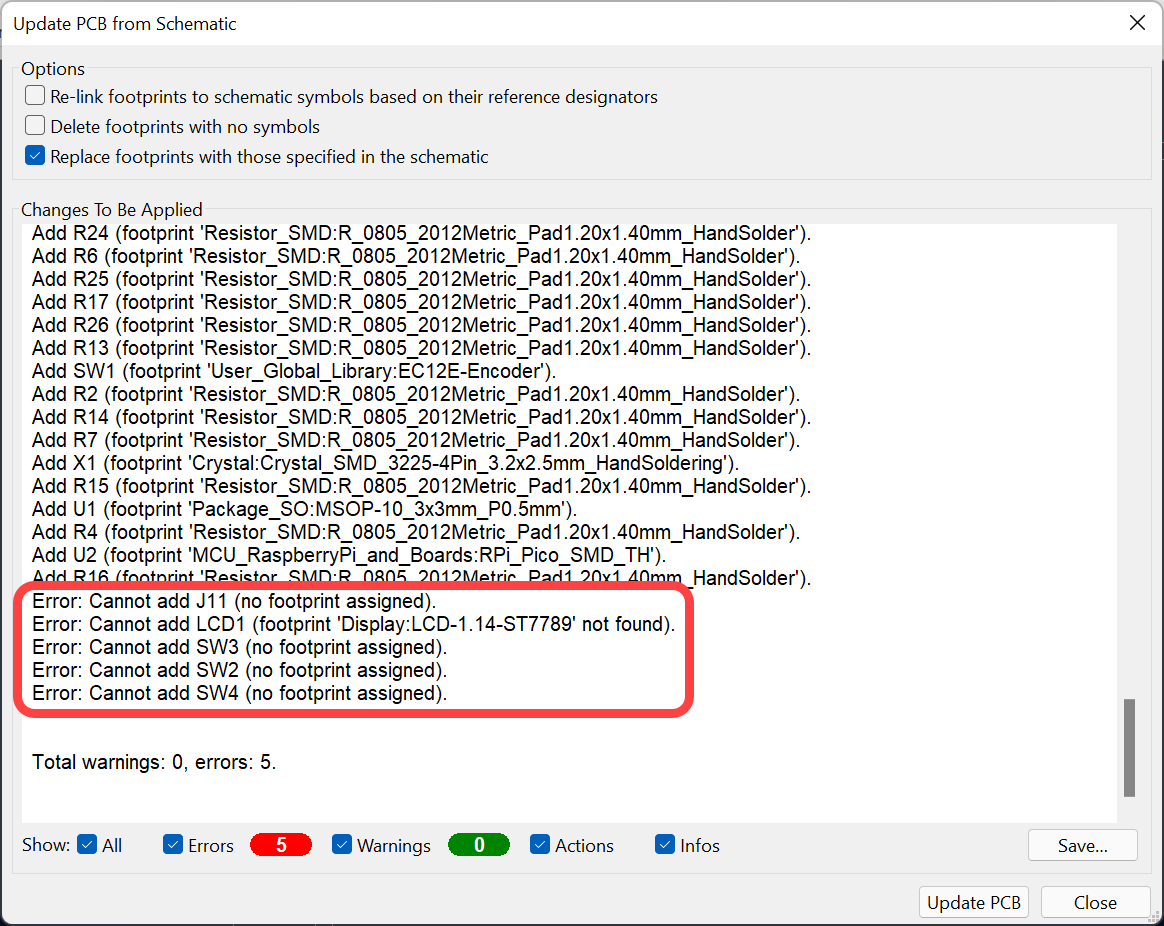
However, it reported that I'd forgotten to assign footprints to five components:
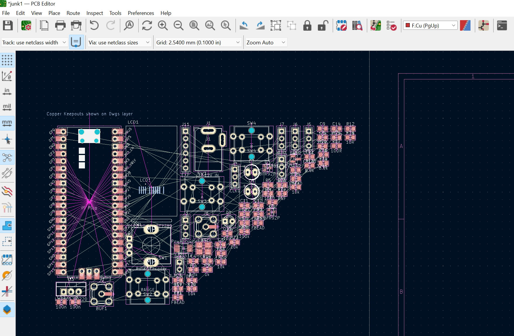
I clicked Close instead of Update PCB, and then went back to the schematic and corrected these errors, and then re-clicked on the Update PCB with changes made to the Schematic icon and then clicked Update PCB - all went fine now, and components appeared : ) I put them to the side of the sheet:
I drew a PCB outline using the Edge.Cuts layer, and then moved the origin to be at one corner of the board, so that I could easily position things that needed to be at specific locations on the board (like buttons and connectors and so on). To move the origin, the menu item Place->Drill/Place File Origin is used, and then click on the location that you wish to be the origin (see the comments below how to set up another origin for relative measurements, since that could be handy too).
A really great feature is the 'M' key. To use it, click on a component (I has to click on the edge of components to not select a pad since I wanted to select the entire component - this is a bit annoying, I've not found a solution yet although I'm sure it must exist) and then once you've released the mouse button, press the 'M' key and the component will stick to the cursor so you can move it around without having to keep the mouse button depressed. Click again to drop the component at the new cursor position. The brilliant part of the M feature is that it automatically aligns to the grid, and it aligns either pads or the center of the component - really neat! Just move your mouse close to the center of the component feature that you wish to align before your press M. What this means is that if you're trying to align multiple parts, you can choose if you want to align using the component centers, or the component pins. EAGLE didn't have this feature, and my workaround in EAGLE was to use its footprint editor and set the origin of the component to the most likely location that needed centering, and then hope that no board needed different alignment.
The main keys I used were M and R in the PCB Editor (R will rotate the component). F will flip the component onto the other side of the board.
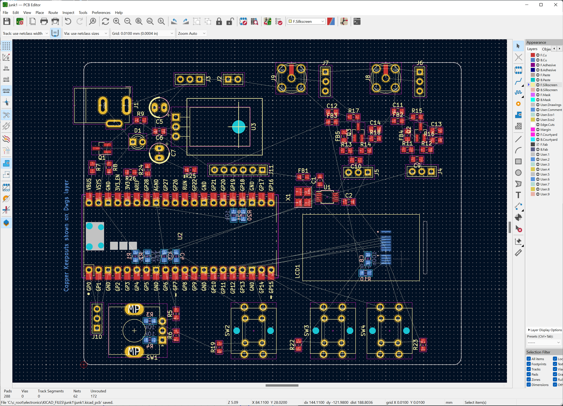
After a first pass, I had the components positioned approximately where I wanted them:
If at any point the circuit needs altering, or footprints need modifying, the procedure is to go into the Schematic editor, make the change there (e.g. double-click on a component to get to the properties and change the footprint) and then save the Schematic, and then go back to the PCB Editor, and click on the the Update PCB with changes made to the Schematic icon and then clicked Update PCB as before. EAGLE automatically did this, whereas, like a lot of PCB CAD programs, unfortunately, it is a manual step in KiCAD. Anyway, I can get used to this change in workflow.
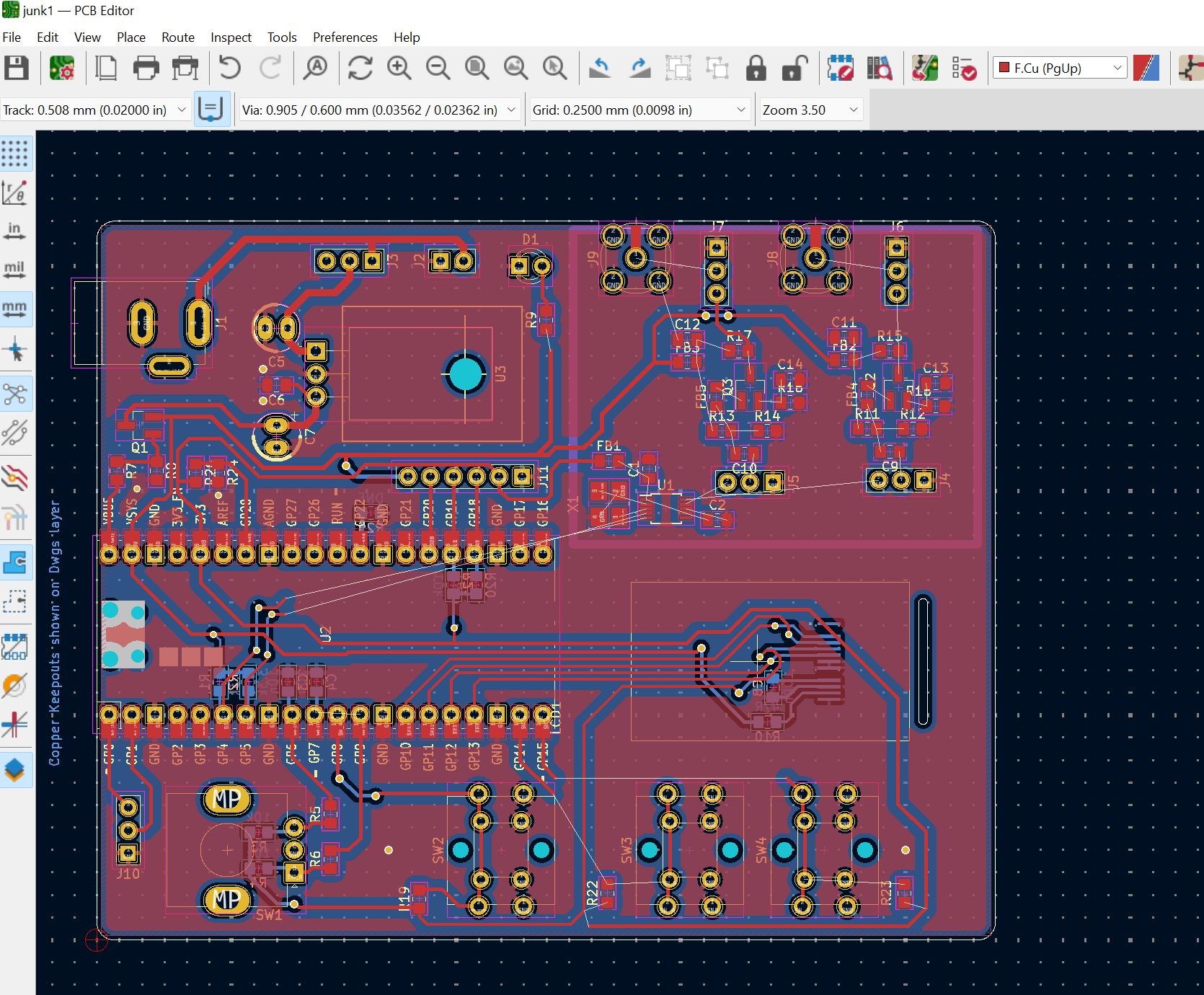
By the end of day 4, I had manually routed a reasonable portion of the board as shown below (first pass - I have to do a second pass to do the tidying up). To do this, the most useful keypresses were X which starts off a trace and V which allows you to place a via and switch layers as you lay down traces. If you want to undo traces, press the Delete button on your keyboard. Copper pours for ground plane were easy, just select the blue Add a Filled Zone icon on the right of the screen, and when you click on a corner, it will prompt you for the net name (e.g. GND) that you wish to use for the copper pour. Once all the corners have been defined, press B to fill it in. As you route the tracks, you'll have to press B again to update the copper pours on the display.
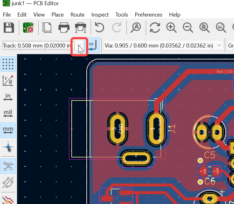
For the track widths, I had to pre-define some values. To do that, click here:
Them, click the little '+' button at the bottom to keep adding all your desired widths and desired via sizes as shown here (I used values which I was using for EAGLE):
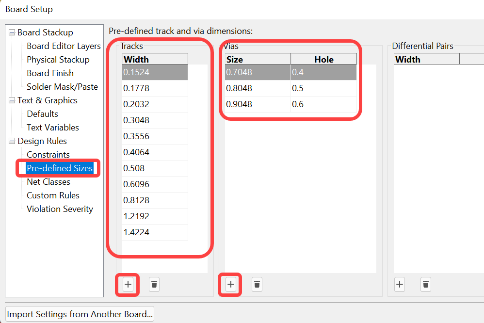
Now you can select these values from the drop-down at any point you wish to change track width. The values are in millimeters, but they get displayed in inches too (and from that it is easy to visually figure out the mils value if desired).
Day 5 - Completing the Board Layout, Design Rule Checks and Generating Gerber Output Files
The interesting feature for today was the trace length matching capability:
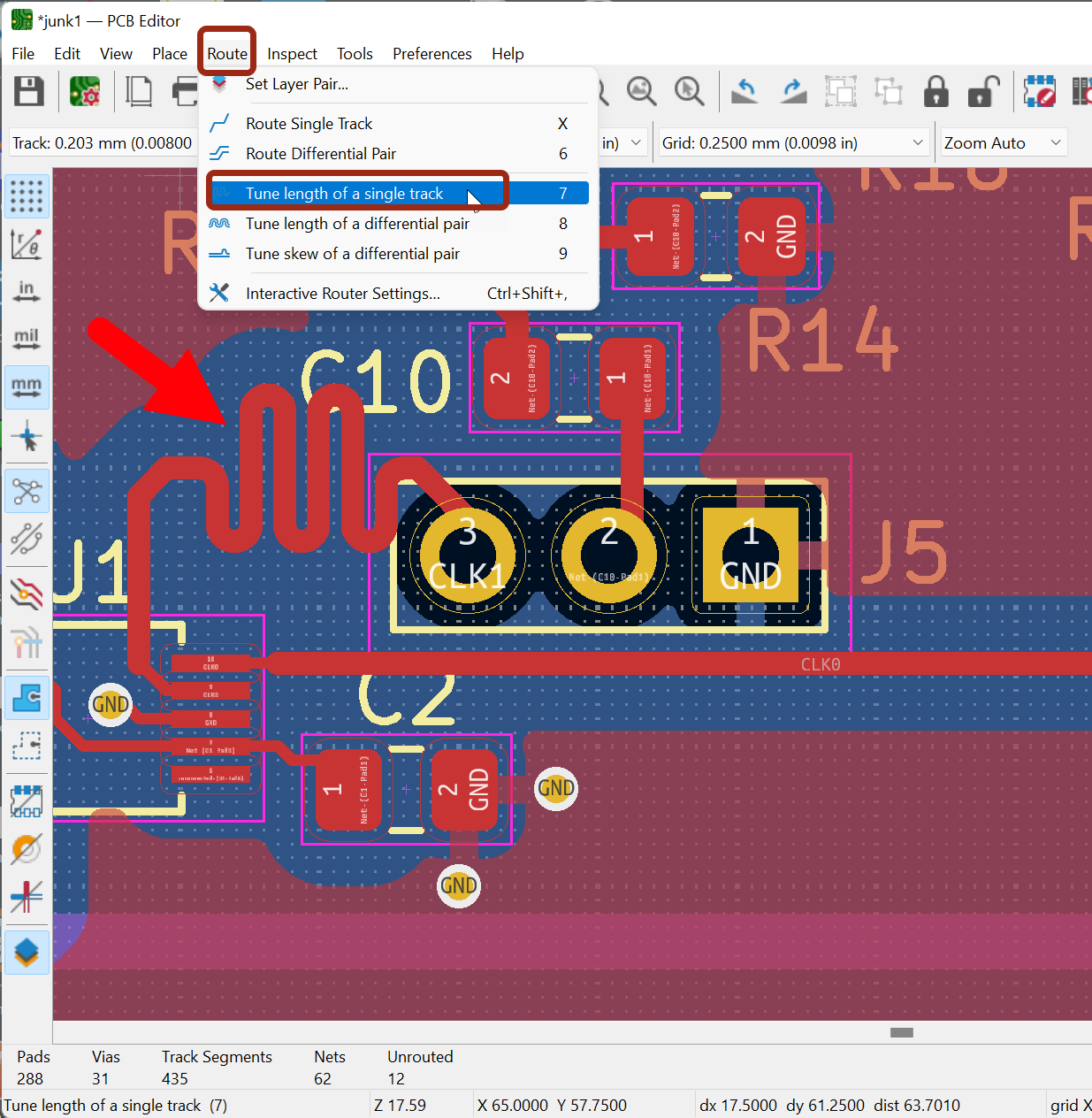
The way it works, is first you examine the trace that you want to match to, and at the bottom the trace length is displayed in millimeters. Next, go to Route->Tune Length of a Single Track, and then click on trace that you want to be matched to the first one. Next, right-click and a menu appears where you can specify the length. Now slide the mouse pointer along the trace, and KiCAD will automatically add the meandering pattern : ) This was very useful because my board has two clock outputs that can require synchronisation.
The Inspect->Design Rules Checker function was used to work through all the errors/warnings. By the end of it, I only had some silkscreen warnings which I examined one-at-a-time to see if it was acceptable visually or not.
The built-in 3D viewer is also handy (click to enlarge the image):
Next, I generated the Gerber files using the File->Plot menu. I followed the JLC PCB website and configured the plot menu as shown here:
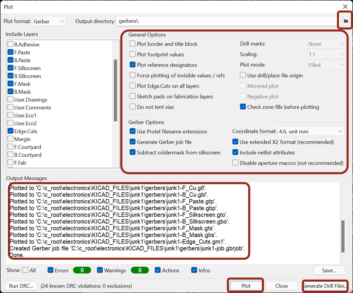
Both Plot and Generate Drill Files need to be clicked. In EAGLE it is all one step. Anyway, when I clicked on Plot, ten files were generated for my 2-layer design. When Generate Drill Files was clicked, another window appeared, and it was configured as shown here:
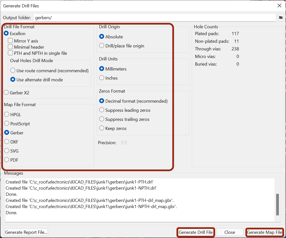
Both Generate Drill File and Generate Map File were clicked, and a total of four more files were generated.

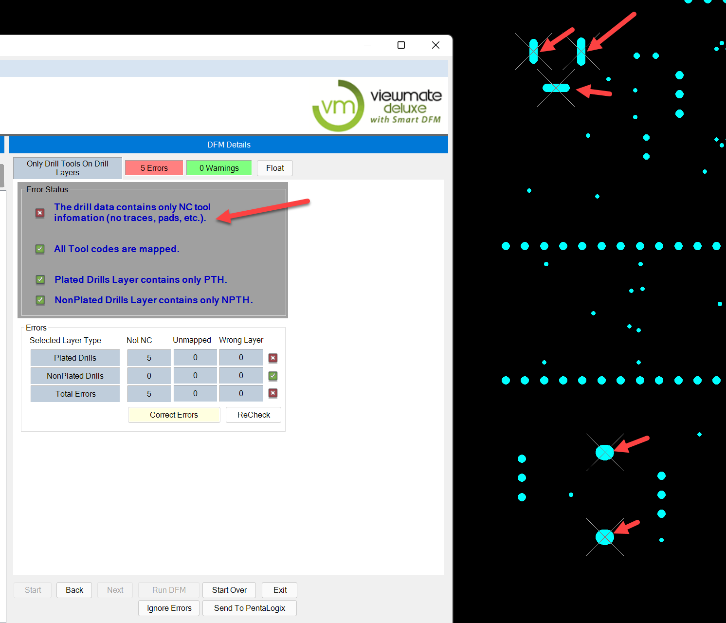
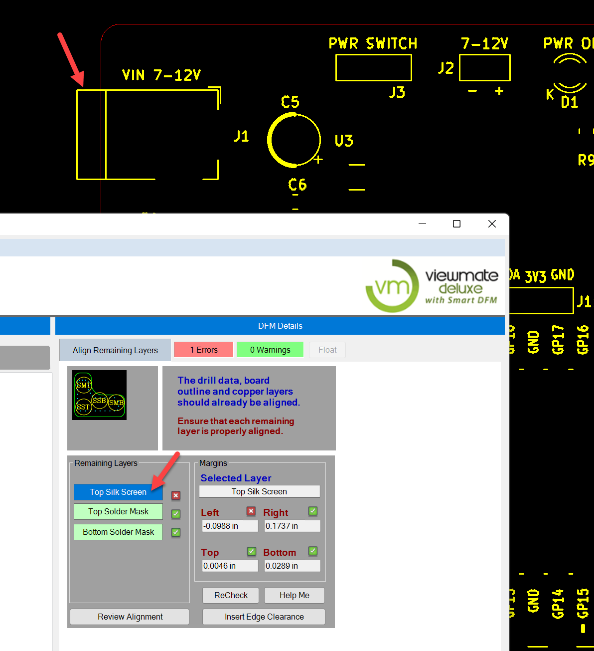
I then examined the files using ViewMate. It found these issues:
(a) The board outline layer contained non-plated slots/shapes that I had in one of the components. This is because I created a component with a shaped slot in the Edge.Cuts layer. I think this is OK, this is what I did in EAGLE and JLC PCB had no issue with that with my EAGLE generated files, so I am going to ignore this error.
(b) The drill file contained oval holes. I don't know what to do about this. JLC PCB KiCAD guidelines suggest this is how it should be, but I've always used a separate file with EAGLE to indicated routed holes. I will ignore this, and see what comes back from the PCB factory. The screenshot below shows my 5 oval holes that generated 5 errors in Viewmate.
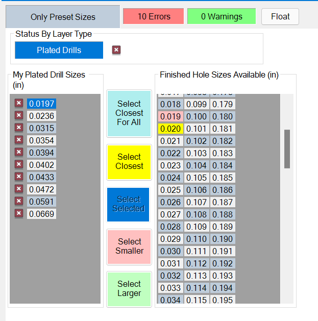
(c) Viewmate didn't like the drill sizes. I'm fairly sure I can safely ignore these; JLC PCB will simply pick the closest drills they have.
(d) I had silkscreen off the board edge. Safe to ignore.
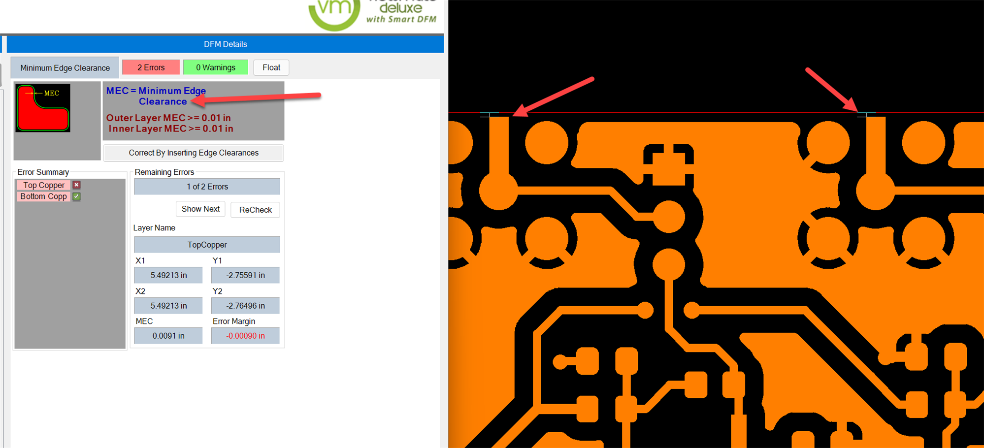
(e) I have copper too close to the board edge, at two locations. Ordinarily, this isn't good, but I am going to ignore this because this was deliberate, I have done it before on these connector pads, and it's perfectly fine on such large pads, at least for basic prototypes.
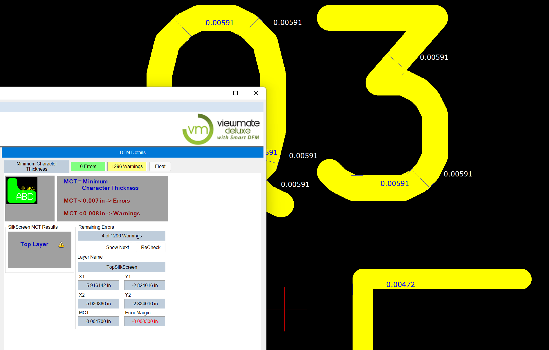
(f) A total of 1296 warnings for the silkscreen, concerning width : ) And a few dozen more concerning character spacing.
These are safe to ignore, but for future boards I will consider slightly increasing the thickness to improve readability.
And that's it! The only one area of concern is item (b) since that's new to me, I never had shaped plated holes in a drill file before, it's not the way I did it with EAGLE. Anyway, I'll soon find out when the boards are manufactured.
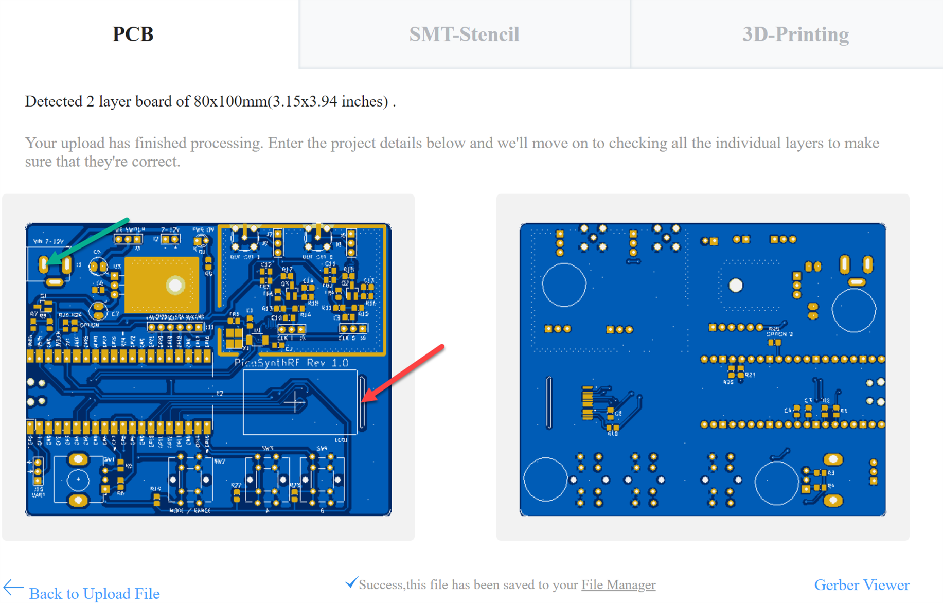
I zipped and uploaded the Gerber files to the JLC PCB website, to see what their automated system thinks of it. The good news is that as shown in the screenshot below, it liked the shaped plated slots (i.e. oval holes), they rendered correctly (indicated with a green arrow). However, the slot in red, which isn't a pad, but is just a cutout, looks odd. However, I'm hoping it is still OK.
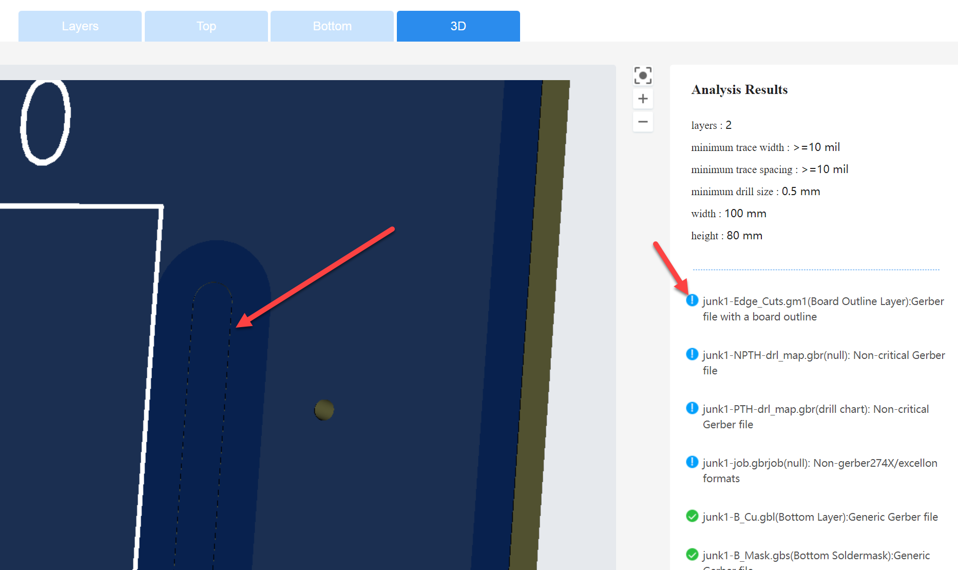
The JLC PCB Gerber viewer indicates a warning on the board outline layer. I will go ahead with it anyway and see what happens when the board is manufactured.
Using Python in the PCB Editor Scripting Console
Now that the board is complete and ordered from the PCB manufacturer, I tried to explore Python scripting for future use. See the discussion below for more information, but in a nutshell here is an example that was written to draw a silkscreen box. To run it, go to Tools->Scripting Console in the PCB Editor, and type:
import sys

print (sys.path)
Then, create a file called box.py with the content below, and place it in one of those folders. I used the folder C:\Users\<your_username>\Documents\KiCad\6.0\scripting\plugins
#
# simple box
#

import sys
import pcbnew

pcb=pcbnew.BOARD()
board = pcbnew.GetBoard()
gd=board.GetDrawings()

def drawline(x1, y1, x2, y2):
    p1 = pcbnew.wxPoint(x1, y1)
    p2 = pcbnew.wxPoint(x2, y2)
    elem = (pcbnew.PCB_SHAPE(board))
    elem.SetLayer(37)  # silkscreen layer
    elem.SetStart(p1)
    elem.SetEnd(p2)
    board.Add(elem)
    pcbnew.Refresh()

def main(width, height):
    hx = (float(width) / 2.0) * 1e6
    hy = (float(height) / 2.0) * 1e6

    cx = 0  # offset, for future use
    cy = 0

    drawline(cx-hx, cx-hy, cx-hx, cx+hy)
    drawline(cx-hx, cx+hy, cx+hx, cx+hy)
    drawline(cx+hx, cx+hy, cx+hx, cx-hy)
    drawline(cx+hx, cx-hy, cx-hx, cx-hy)


if __name__ == "__main__":
    if len(sys.argv) != 3:
        print("Usage ", __file__, "<width> <height>", file=sys.stderr)
        sys.exit(1)
    main(sys.argv[1], sys.argv[2], sys.argv[3])
Now the code can be run by typing these two lines (replace width and height with the desired values):
import box
box.main(width, height)
It will draw a silkscreen box with center at origin (0,0), ready for editing or moving with the mouse.
This is a very simple example, but it's a start. The KiCAD forum has a External Plugins section with useful discussion in this area too.